As electronics continue their relentless march toward Miniaturization, High-density Interconnect (HDI) technology has become standard practice rather than exotic exception. And at the heart of every HDI design lies the Microvia—those laser-drilled, small-diameter vias that make the interlayer connections possible within the tight routing channels of fine-pitch BGA fanouts and ultra-compact layouts.
But a Microvia is not just a microvia. How you place these vias relative to each other—particularly when multiple Microvias must span more than one layer—has profound implications for reliability, Signal Integrity, fabrication cost, and yield. The two fundamental approaches, staggered and stacked Microvias, represent different philosophies of interconnect architecture, and choosing between them is one of the most consequential decisions in HDI design.
This article examines both approaches in depth, exploring their mechanical, electrical, and economic tradeoffs so you can make informed decisions for your next HDI project.

Understanding Microvia Fundamentals
Before comparing placement strategies, it is essential to understand what makes microvias different from conventional through-hole vias.
What Defines a Microvia
A microvia is typically defined as a via with a diameter of 0.15mm (6 mil) or less, spanning only one layer of the board—connecting an outer layer to the immediately adjacent inner layer (or two adjacent inner layers in some constructions). Microvias are created by Laser Drilling rather than mechanical drilling, which allows their small diameter and eliminates the mechanical stress that drill bits impose on the laminate.
Key microvia characteristics:
- Diameter: Typically 0.10-0.15mm (4-6 mil), though some advanced processes achieve 0.075mm (3 mil)
- Depth: One layer span (typically 0.05-0.10mm dielectric thickness)
- Aspect ratio: Usually 0.5:1 to 1:1—significantly lower than through-hole vias, which enables reliable plating
- Formation method: CO2 laser, UV laser, or combined UV/CO2, depending on the Dielectric Material and whether the copper foil is penetrated by the laser or opened by a separate etch step
Why Microvias Span Only One Layer
The low aspect ratio of microvias is both their strength and their constraint. A 0.10mm diameter via spanning a 0.10mm dielectric has an aspect ratio of 1:1, which plating chemistry can reliably fill. A 0.10mm via spanning two layers (0.20mm total dielectric) would have a 2:1 aspect ratio—still platable but with lower reliability and higher risk of voids in the plating. This single-layer-span constraint is what makes multi-layer interconnect strategies—staggered and stacked—necessary.
Staggered Microvias: The Conservative Approach
In a staggered microvia arrangement, two (or more) microvias that together span multiple layers are offset horizontally from each other. The first microvia connects layer 1 to layer 2; the second microvia, offset to a different position on layer 2, connects layer 2 to layer 3. A short trace on layer 2 connects the two vias, completing the path from layer 1 to layer 3.
How Staggered Vias Are Constructed
The fabrication process for staggered microvias follows the standard HDI Sequential Lamination flow:
- First build-up: The core (inner layers) is laminated with the first build-up dielectric and copper foil. Laser Drilling creates the first set of microvias (e.g., L1-L2). These vias are plated and the L1 copper pattern is etched.
- Second build-up: Another dielectric layer and copper foil are laminated over the first build-up. Laser drilling creates the second set of microvias (e.g., L2-L3), positioned offset from the L1-L2 vias. These vias are plated and the L2 pattern is etched, including the short traces connecting the staggered via pairs.
- Subsequent build-ups: The process repeats for additional layers.
Because each microvia spans only one dielectric layer, every via has a favorable aspect ratio for reliable plating. The connecting traces on intermediate layers are created during normal patterning—no special process steps are required.
Advantages of Staggered Microvias
- Superior plating reliability: Every microvia has an aspect ratio of approximately 1:1 or less, which is the regime where electroless and electrolytic Copper Plating are most reliable. Void-free plating is readily achieved with standard process parameters.
- No via-on-via alignment risk: Because the vias are offset, there is no requirement for precise layer-to-layer alignment at the via location. Misregistration between build-up layers affects the connecting trace length but does not compromise the via structure itself.
- Better thermal reliability: During thermal cycling, each microvia expands and contracts independently. There is no concentrated stress point where two vias overlap. This makes staggered vias the preferred choice for applications with demanding thermal cycling requirements (automotive, aerospace, industrial).
- Lower fabrication risk: The staggered approach uses standard Sequential Lamination with no special processing requirements. Every fabrication step is well-characterized and high-yield.
- Easier inspection and failure analysis: If a staggered via connection fails, the failure can be isolated to one of the individual microvias or the connecting trace. Cross-section analysis is straightforward because the vias are in different locations.
Disadvantages of Staggered Microvias
- Consumes more routing area: The horizontal offset between staggered vias requires more board area than a stacked arrangement. In BGA fanouts where routing space is critically tight, this area penalty can force wider channel spacing or additional layer pairs.
- Longer interconnect length: The connecting trace on the intermediate layer adds length—and therefore inductance—to the interconnect path. For very high-speed signals (above 10 Gbps), this additional inductance can degrade Signal Integrity.
- Additional trace on intermediate layer: The connecting trace consumes routing resources on the intermediate layer, potentially blocking channels that would otherwise be available for other signals.
- Higher via count: For multi-layer spans, staggered vias require more total vias than stacked vias (two vias and a trace versus one stacked structure spanning two layers).
Stacked Microvias: The Aggressive Approach
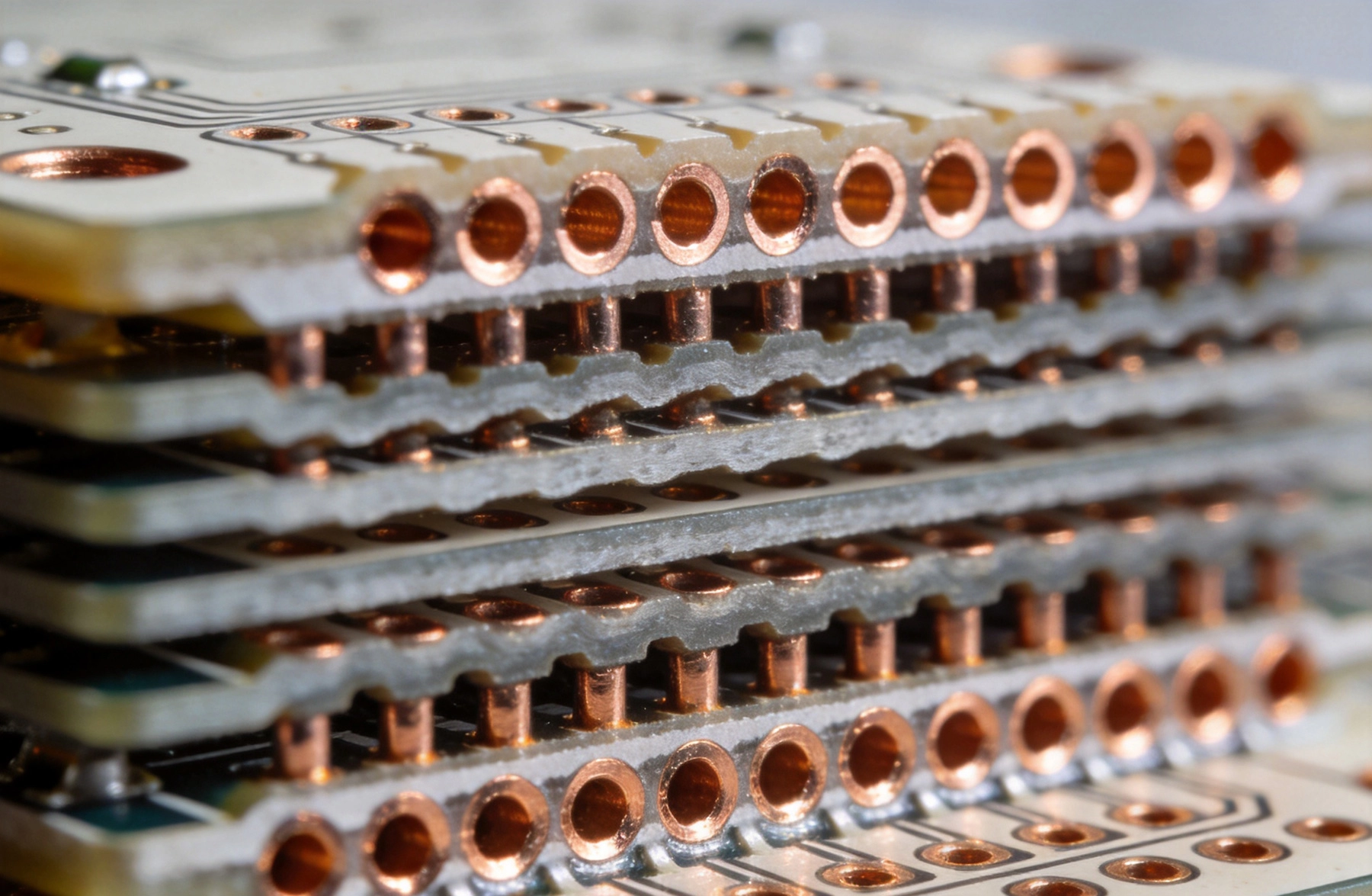
In a stacked microvia arrangement, microvias on adjacent layer pairs are placed directly on top of each other—vertically aligned so that the pad of the lower microvia serves as the capture pad for the upper microvia. A pair of Stacked Microvias creates a direct vertical connection spanning two dielectric layers without any intermediate trace.
How Stacked Vias Are Constructed
The fabrication of Stacked Microvias requires more process control than staggered vias:
- First build-up: Microvias (L1-L2) are laser-drilled, plated, and filled with a conductive material—either Copper Plating (copper-filled microvia) or epoxy fill followed by copper planarization. The fill is critical: the upper microvia will be drilled on top of this filled via, and the fill must provide a flat, solid, conductive base.
- Planarization: The filled microvias are planarized (surface-leveled) to create a flat copper surface. Any residual Dielectric Material or uneven plating at the via location will cause defects in the upper microvia.
- Second build-up: The next dielectric and copper foil are laminated. Laser drilling creates the L2-L3 microvias directly aligned over the filled L1-L2 vias. Because the lower vias have been filled and planarized, the laser can reliably drill through the copper foil and dielectric to the copper fill of the lower via.
- Plating and patterning: The L2-L3 microvias are plated and the outer layer pattern is etched.
The key process requirement is Via Filling and planarization. Without a properly filled and flat lower via, the upper microvia may drill into a void, creating an open circuit, or the lamination may trap air in the overlap zone, creating a reliability hazard.
Advantages of Stacked Microvias
- Minimal routing area: Stacked vias occupy the smallest possible board footprint—a single pad location. This is critically important in Bga Fanout routing where via channels are the limiting factor on routing density.
- Shortest interconnect path: The vertical stacking eliminates the intermediate connecting trace, minimizing total interconnect length and inductance. For high-speed signals, this translates directly to better signal integrity.
- No intermediate layer routing consumed: The intermediate layer is not occupied by a connecting trace, freeing routing channels for other signals.
- Lower parasitic inductance: The elimination of the connecting trace and its associated current loop reduces the parasitic inductance of the interconnect. For power delivery networks in high-performance computing, this inductance reduction can be significant.
Disadvantages of Stacked Microvias
- Higher fabrication complexity and cost: Via Filling (copper or epoxy) and planarization are additional process steps that add cost and cycle time. Copper-filled microvias require extended plating times and careful process control to achieve void-free fills.
- Alignment sensitivity: The upper microvia must be drilled precisely over the filled lower via. Registration errors between build-up layers can cause the upper via to partially miss the lower via fill, creating a high-resistance connection or an open. This risk increases with board size and layer count.
- Concentrated thermal stress: During thermal cycling, the stacked via structure experiences concentrated stress at the interface between the two microvias. The coefficient of thermal expansion (CTE) mismatch between the copper fill, the surrounding dielectric, and the plating creates stresses that can cause cracking or delamination at the via-to-via interface over time.
- Lower reliability under thermal cycling: Multiple industry studies have demonstrated that stacked microvias exhibit higher failure rates than staggered microvias under accelerated thermal cycling. The failure mode is typically cracking at the via-to-via interface or delamination within the via fill. IPC-6012 Class 3 applications (aerospace, medical, automotive safety) often mandate staggered vias or require special qualification of stacked via structures.
- More difficult failure analysis: When a stacked via connection fails, determining which of the stacked vias caused the failure requires destructive cross-section analysis. The failure may be at either via interface or within the fill material—diagnosis is more complex than for staggered vias.
Head-to-Head Comparison: Key Decision Factors
Reliability Under Thermal Cycling
This is the most critical differentiator. Extensive testing—by OEMs, academic researchers, and IPC working groups—consistently shows that staggered microvias outperform stacked microvias in thermal cycling reliability. The concentrated stress at the stacked via interface is the root cause.
Typical test results (thermal cycling -40°C to +125°C, per IPC-TM-650 Method 2.6.7):
- Staggered microvias: Mean cycles to failure typically exceeds 1000 cycles, with Weibull characteristic life above 1500 cycles.
- Stacked microvias: Mean cycles to failure typically 400-800 cycles, with Weibull characteristic life 600-1200 cycles. Results vary significantly with via fill quality and plating parameters.
For applications with more than 500 expected thermal cycles over the product lifetime, staggered vias are strongly recommended. For consumer electronics with benign thermal environments and limited product lifetime (3-5 years), stacked vias may be acceptable.
Signal Integrity at High Speed
For signals operating below 5 Gbps, the difference in signal integrity between staggered and stacked vias is negligible—the additional inductance of the staggered via connecting trace is small relative to other discontinuities in the signal path. Above 5 Gbps, and especially above 10 Gbps, the stacked via advantage becomes measurable:
- Inductance: A typical staggered via pair with a 0.5mm connecting trace adds approximately 0.1-0.2 nH of inductance compared to a stacked via pair. At 10 GHz, this represents an impedance discontinuity of approximately 6-12 ohms—enough to cause measurable return loss degradation.
- Return path continuity: Stacked vias provide a more symmetric return path for differential pairs transitioning between layers, reducing mode conversion and common-to-differential conversion.
For high-speed serial links (PCIe Gen3/4, USB 3.x, 10GbE), stacked vias in the Bga Fanout region can provide a measurable signal integrity benefit. For slower signals, this benefit does not justify the reliability tradeoff.
Routing Density in BGA Fanouts
This is where stacked vias shine. In a fine-pitch BGA fanout (0.4mm or 0.5mm pitch), the via channel width—the space available for routing between adjacent via pads—is the fundamental constraint on how many signals can escape per layer pair. Stacked vias, by occupying only one pad location instead of two (or more) offset pad locations, free up routing channels.
The practical impact depends on the BGA pitch and the via pad size:
- 0.8mm pitch and above: Routing density is usually not the limiting factor—either staggered or stacked vias work without density issues.
- 0.5mm pitch: Staggered vias may require additional layer pairs to route all signals; stacked vias can often achieve the same escape routing with fewer layers.
- 0.4mm pitch: Stacked vias are almost mandatory for efficient fanout routing. Staggered vias at this pitch consume so much routing area that the layer count penalty becomes prohibitive.
Fabrication Cost and Yield
Stacked vias cost more than staggered vias due to:
- Via fill process (copper plating or epoxy fill): $0.01-0.03 per via
- Planarization process: included in fill cost at most fabricators
- Reduced yield from alignment sensitivity: typically 1-3% lower yield for stacked via designs
For a board with 500 microvias, the via fill cost adds approximately $5-15 per board. This is modest for high-value boards but noticeable for cost-sensitive consumer products. The yield penalty, while small, compounds with other yield factors and can become significant for complex boards with many stacked via locations.
Hybrid Approaches: Best of Both Worlds
In practice, many HDI designs do not choose exclusively between staggered and stacked vias—they use both, applying each strategy where its advantages are most valuable.
Stacked Vias in BGA Fanout, Staggered Elsewhere
The most common hybrid approach uses stacked microvias in the BGA fanout region—where routing density is critical and the signal paths are short—and staggered microvias everywhere else on the board. This captures the routing density benefit of stacked vias where it matters most while using the more reliable staggered approach for the majority of the board area.
Stacked Vias for High-Speed Signals, Staggered for Power
Another strategy uses stacked vias for high-speed signal transitions (where the inductance benefit matters) and staggered vias for power and ground connections (where current capacity and thermal cycling reliability are more important). Power and ground vias typically have more routing space available and do not benefit from the area savings of stacking.
Skip Vias as a Middle Ground
A skip via is a microvia that spans two dielectric layers in a single drilling step—creating an L1-L3 connection directly without an intermediate via on L2. Skip vias have an aspect ratio of approximately 2:1, which is higher than single-layer microvias but lower than through-hole vias. They provide the area savings of stacked vias (single pad location) without the via-on-via alignment risk. However, skip vias require special plating parameters and are not supported by all fabricators. They represent a useful option when available—particularly for 1+2+1 HDI constructions where the skip via eliminates the need for staggered via pairs or stacked structures.
Design Guidelines: Choosing the Right Strategy
The choice between staggered and stacked microvias should be driven by your application's specific requirements, not by default design rules or habit. Here are decision guidelines organized by application type:
Consumer Electronics (Smartphones, Tablets, Wearables)
- Thermal cycling severity: Low to moderate (0-70°C typical range)
- Product lifetime: 2-5 years
- BGA pitch: Often 0.4mm
- Recommendation: Stacked vias are appropriate. The routing density benefit is critical, and the thermal cycling requirements are benign enough that stacked via reliability is acceptable. Use Via-in-pad with copper fill.
Telecommunications and Networking
- Thermal cycling severity: Moderate (0-85°C, some field cycling)
- Product lifetime: 7-15 years
- BGA pitch: 0.5-0.8mm
- Recommendation: Hybrid—stacked vias for high-speed BGA fanouts (PCIe, Ethernet SERDES), staggered vias elsewhere. Ensure the fabricator has a proven stacked via process with reliability data.
Automotive (ADAS, Infotainment, Body Electronics)
- Thermal cycling severity: Severe (-40°C to +125°C, thousands of cycles)
- Product lifetime: 10-15 years
- BGA pitch: 0.5-0.8mm
- Recommendation: Staggered vias are strongly preferred for Class 3 (safety-critical) applications. For non-safety applications, stacked vias may be acceptable with qualification data demonstrating adequate thermal cycling performance. AEC-Q200 reliability testing should be considered.
Aerospace and Defense
- Thermal cycling severity: Very severe (-55°C to +125°C, extreme cycling)
- Product lifetime: 15-30+ years
- BGA pitch: 0.8-1.0mm (typically coarser pitch packages)
- Recommendation: Staggered vias are the only appropriate choice. The thermal cycling severity and lifetime requirements are incompatible with the known reliability limitations of stacked microvias. Most aerospace and defense specifications explicitly mandate staggered vias.
Medical Devices (Implantable and Life-Critical)
- Thermal cycling severity: Moderate to severe (body temperature cycling plus sterilization cycles for external devices)
- Product lifetime: 5-15+ years (implantable devices must not fail)
- Recommendation: Staggered vias are required. The zero-failure tolerance for implantable devices makes stacked vias unacceptable. For non-implantable medical devices, the same automotive guidelines apply—staggered preferred, stacked acceptable with qualification for non-critical applications.
Working With Your Fabricator: Process Capabilities Matter
Your choice of microvia placement strategy must be informed by your fabricator's actual capabilities—not their marketing claims. Key questions to ask:
- What is your maximum registration accuracy between sequential build-up layers? This determines the safe margin for stacked via alignment. If registration is ±25 µm, a stacked via with a 0.15mm pad leaves 50 µm of pad after worst-case misregistration—tight but functional. If registration is ±50 µm, stacked vias become significantly riskier.
- What via fill process do you use, and what fill quality data can you provide? Copper-filled vias are superior to epoxy-filled vias for stacked structures because copper provides a homogeneous, highly conductive fill with no Cte Mismatch at the interface. Request cross-section micrographs showing typical fill quality.
- What thermal cycling data do you have for stacked microvia structures? A fabricator who has invested in stacked via capability should have reliability test data demonstrating performance under thermal cycling. If they do not have this data, they are not qualified for stacked via production in demanding applications.
- What is your yield on boards with stacked vias versus staggered vias? Ask for production yield data on comparable board complexity. A 1-3% yield penalty for stacked vias is normal; a 5%+ penalty suggests process issues.
Future Trends: Where Microvia Technology Is Heading
Any-Layer HDI
Any-layer Hdi (also called ELIC—every layer interconnect) allows microvias between any two adjacent layers in the stackup, not just between the outer layers and the first inner layer. This enables via structures that were previously impossible and changes the staggered/stacked tradeoff by providing more routing flexibility. Any-layer Hdi is increasingly available from advanced fabricators but remains significantly more expensive than traditional HDI.
Improved Via Fill Materials
Research into novel via fill materials—including copper alloys with improved ductility and ceramic-copper composites with matched CTE—aims to reduce the thermal cycling vulnerability of stacked vias. If these materials prove reliable, they could close the reliability gap between stacked and staggered structures.
Microvia Reliability Standards Evolution
IPC is actively developing more detailed reliability test methods and acceptance criteria specific to microvia structures. IPC-6012 (the rigid board qualification standard) and IPC-TM-650 (test methods) are being updated with microvia-specific requirements that will formalize the reliability expectations for both staggered and stacked vias. Designers should monitor these standards developments and align their qualification programs accordingly.
Conclusion
The choice between staggered and stacked microvias is not a simple either/or—it is a design decision that balances routing density, signal integrity, fabrication complexity, cost, and reliability. Staggered vias offer superior reliability and simpler fabrication at the cost of routing area and interconnect length. Stacked vias provide maximum routing density and minimum parasitic inductance but carry reliability risks that limit their suitability for demanding applications.
For most HDI designs, the optimal approach is a hybrid one: stacked vias where routing density or signal integrity demands them (typically BGA fanouts and high-speed signal transitions), and staggered vias everywhere else. This pragmatic strategy captures the benefits of both approaches while limiting the reliability exposure of stacked structures to the areas where they are truly needed.
Whatever strategy you choose, validate it against your fabricator's capabilities and your application's reliability requirements. The most elegant via architecture in CAD becomes a liability in production if the fabricator cannot execute it reliably or the thermal environment exceeds the structure's capability. Design for the real world—not just the virtual one.