
Programmable Logic Controllers and motor drives form the operational backbone of modern industrial automation. These systems monitor processes, execute control algorithms, and drive motors with millisecond precision across manufacturing floors that operate around the clock. When a PLC in an automotive assembly plant goes down, production stops. When a motor drive fails in a water treatment facility, critical processes halt. The reliability expectations placed on these systems demand Electronics Manufacturing approaches that go beyond standard PCB Fabrication—demands that High-density Interconnect (HDI) technology is uniquely positioned to meet.
HDI solutions offer industrial equipment manufacturers the ability to pack more functionality into smaller form factors while improving Signal Integrity, Thermal Performance, and long-term reliability. This article explores how Hdi Technology applies to PLCs and motor drives, why HDI construction improves reliability in demanding industrial environments, and how to implement HDI solutions that meet the exacting standards of industrial automation equipment.
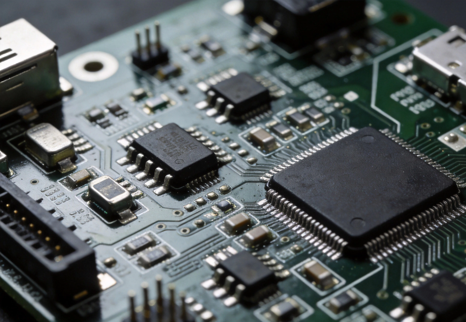
Industrial environments present electronics with stresses that consumer and commercial applications rarely encounter. Understanding these challenges helps explain why Hdi Technology has become increasingly important in PLC and motor drive design.
Industrial equipment operates in environments ranging from unheated warehouses to foundry floors with ambient temperatures exceeding 50°C. Beyond ambient conditions, internal heat generation from power semiconductors, processors, and passive components creates significant thermal gradients within enclosed enclosures. PLCs and motor drives experience thousands of thermal cycles over their service life, each cycle stressing solder joints, plated through-holes, and component interfaces.
For equipment expected to operate reliably for 10 to 20 years with minimal maintenance, the cumulative effect of thermal cycling becomes a primary failure mechanism. Boards that develop cracks at vias, delaminate at layer interfaces, or experience solder joint fatigue create intermittent failures that are difficult to diagnose and costly to remediate.
Motors generate vibration that transmits through mounting structures to nearby electronics. Large contactors and electromagnetic devices create momentary mechanical shocks during switching. Conveyors, presses, and other equipment vibrations find their way into electronic enclosures. This mechanical stress attacks solder joints, connector interfaces, and board-level interconnections in ways that thermal stress alone would not.
HDI construction with its improved layer-to-layer connections and tighter tolerances for component placement helps resist mechanical stress by minimizing stress concentration points. The mechanical robustness of well-designed Hdi Boards contributes directly to the Vibration Resistance that industrial equipment demands.
Industrial facilities are electrically noisy environments. Motor starting currents create voltage sags and transients. Variable frequency drives generate conducted and radiated EMI across a wide spectrum. Welding equipment, switching power supplies, and fluorescent lighting inject noise into shared power distribution systems. PLCs must process sensor inputs accurately despite this interference. Motor drives must switch kilowatts of power without corrupting their own control signals.
HDI construction with its controlled impedance features, systematic ground plane design, and superior signal routing enables the clean Signal Integrity that reliable industrial control requires. The ability to route sensitive signals in inner layers between solid reference planes reduces susceptibility to external noise sources.
High-density Interconnect technology encompasses a range of PCB construction techniques that enable higher routing density, improved electrical performance, and increasingly sophisticated layer-to-layer connectivity compared to traditional through-hole designs.
The defining characteristic of HDI is the Microvia—small laser-drilled vias typically 100 to 200 microns in diameter that connect adjacent layers. Compared to mechanically drilled through-holes of 300 microns or larger, Microvias consume dramatically less board real estate, allowing more routing channels and more efficient use of available area.
For PLC and motor drive applications, Microvia Technology enables dense routing of control signals around power components without the routing congestion that plagues traditional board designs. The reduced via stub length of stacked Microvias also improves signal integrity for high-speed control signals by minimizing stub resonances.
Advanced HDI constructions like Any-layer Hdi (ALH) allow vias to connect any two layers in the stackup, not just adjacent layers. This flexibility enables highly efficient routing where signals can take the most direct path without routing around obstacles created by previous layer designs.
For motor drives with complex control sections that must route high-speed encoder signals, PWM outputs, and communication buses through a dense area, any-layer interconnection provides routing options that simply do not exist with traditional layer-pair via technology.
Hdi Boards handle fine-pitch components with greater ease than traditional boards. The improved registration accuracy of HDI fabrication—typically ±50 microns or better compared to ±100 microns for standard boards—enables reliable placement of 0.4 mm pitch QFNs, fine-pitch BGAs, and other dense component packages that increasingly appear in modern PLCs and motor drives.
Modern PLC processors and communication ICs often come in BGA packages with 0.8 mm or 0.65 mm pitch that benefit from HDI board characteristics. Motor drive gate drivers and current sensing ADCs in fine-pitch packages similarly require HDI-quality fabrication for reliable assembly.
Selecting the appropriate Hdi Stackup depends on the specific requirements of the PLC or motor drive application. Different configurations offer different trade-offs between routing density, electrical performance, Thermal Management, and cost.
Type III HDI—featuring Stacked Microvias over Buried Vias—provides the highest routing density available. A typical Type III stackup for a complex PLC processor board might use 8 to 10 layers with Microvia layers at the surface and stacked connections through the full depth of the board. This construction supports the most aggressive component density while maintaining excellent electrical performance.
For PLCs with multiple processors, large FPGAs or ASICs, and extensive communication interfaces, Type III HDI enables routing all signal layers without sacrificing ground plane integrity or creating routing bottlenecks that would compromise signal quality.
Type II HDI—with stacked microvia layers over traditional Buried Vias—offers a balanced approach between density and cost. This configuration works well for motor drive control sections that combine high-density digital circuitry with power components requiring larger pad sizes and heavier copper.
A Type II stackup for a motor drive controller typically uses 6 to 8 layers, with microvia layers supporting fine-pitch digital components and traditional through-vias connecting to larger pad areas for power components. This mixed approach optimizes the board for both control and power functions without requiring the full complexity of Type III construction.
HDI boards can be built with traditional cores—rigid fiberglass sections with copper on both sides—or with coreless construction where layers are built up on a carrier without rigid core material. Coreless construction offers the highest routing density but requires more sophisticated manufacturing processes.
For industrial PLC and motor drive applications, core-based HDI construction typically provides the best balance of density, reliability, and manufacturing robustness. The core provides mechanical stability that benefits long-term reliability in industrial environments. Coreless construction may be considered for the most space-constrained applications where its density benefits outweigh the manufacturing complexity trade-offs.
Managing heat in dense HDI designs for PLCs and motor drives requires careful attention to thermal paths from hot components through the board structure to ambient air or enclosure cooling.
Thermal Vias under processors, FPGAs, and power semiconductors provide the primary thermal path from these heat sources through the board. For HDI designs, thermal via arrays should use the microvia drill size for the most efficient thermal transfer while maintaining adequate spacing to prevent manufacturing defects.
A thermal via array under a BGA Thermal Pad might use 200-micron vias on 1 mm pitch—smaller than standard thermal via practices but well within HDI fabrication capabilities. The small via diameter minimizes the impact on routing channels while still providing effective thermal connection to internal planes.
HDI designs for motor drives typically incorporate heavy copper layers for power distribution alongside high-density signal routing layers. These heavy copper planes serve dual purposes: carrying high currents and distributing heat from power components to the board edges where it can dissipate into the enclosure.
A practical approach uses alternating thin-dielectric high-density layers for signal routing and thicker-dielectric heavy copper layers for power distribution. This combination achieves the routing density HDI provides while maintaining the current-carrying capacity and thermal spreading that motor drive applications require.
For the highest power density, HDI designs can incorporate thin metal core or metal-backed sections that provide superior Thermal Conductivity compared to standard dielectric materials. While more expensive than all-organic constructions, embedded metal cores or Thermal Vias to metal cores under hot components significantly improve Thermal Performance for motor drive applications where power density is critical.
Industrial control systems process signals with accuracy requirements that demand excellent signal integrity. HDI construction supports signal integrity goals through controlled impedance routing, systematic ground plane design, and minimized discontinuities.
HDI technology enables tighter tolerance on trace width and spacing, supporting controlled impedance designs with ±10% or better Impedance Tolerance. For PLCs transmitting data over high-speed interfaces like Ethernet, USB, or RS-485, controlled impedance is essential to prevent reflections that would corrupt data.
Microstrip and stripline constructions on inner layers with solid reference planes provide the most predictable impedance. HDI's systematic layer structure makes it straightforward to designate specific layers for controlled impedance routing with appropriate dielectric thickness and trace geometry.
Via-in-pad construction—placing vias directly in component pads—reduces the inductive stub that would otherwise extend beyond the signal layer. For high-speed signals like PWM outputs, encoder interfaces, and communication buses, minimizing stub length prevents resonant behavior that would affect signal quality.
With HDI's stacked microvia capability, Via-in-pad construction is well-controlled. The small via diameter and precise registration of laser-drilled microvias maintain pad geometry and solderability even with fine-pitch components, avoiding the registration issues that plagued earlier implementations of via-in-pad technology.
HDI stackups can be designed with systematic separation of power and signal layers. A typical 8-layer Hdi Stackup might dedicate layers 2 and 7 to solid ground planes, layers 3 and 6 to power planes, and layers 1, 4, 5, and 8 to signal routing. This systematic structure ensures every signal layer has an adjacent reference plane, minimizing return path inductance and preventing crosstalk between unrelated signal groups.
HDI construction places different demands on the manufacturing process compared to traditional through-hole boards. Understanding these differences helps in selecting appropriate manufacturing partners and designing for producibility.
The precision requirements of HDI—micron-level registration between layers—demand sophisticated manufacturing equipment and tight process controls. Advanced HDI facilities use laser imaging, Automated Optical Inspection, and statistical process control to maintain the alignment tolerances that HDI requires.
When specifying HDI boards for industrial applications, clearly communicate registration requirements and accept criteria. A reputable HDI manufacturer will provide data demonstrating their process capability for the tolerances your application requires.
Sequential Lamination—the process of building up HDI layers in stages—creates interfaces between material batches that must be free of voids, delamination, and contamination. Void-free lamination is essential for reliable performance over the thermal cycling that industrial equipment experiences.
HDI manufacturers use vacuum lamination, pressure control, and carefully characterized press cycles to achieve void-free results. For critical industrial applications, specify requirements for 100% cross-sectional inspection or ultrasonic scanning of lamination interfaces to verify dielectric integrity.
Many industrial PLCs and motor drives use conformal coating to protect against moisture and contamination in harsh environments. HDI constructions with their fine features and multiple dielectric layers must be compatible with the coating process—materials that fill voids poorly or create coating stress at layer interfaces can cause reliability problems.
Specify conformal coating requirements to the HDI manufacturer during design. Acrylic, urethane, and silicone coatings are generally compatible with standard HDI constructions, but specific material combinations and application processes should be qualified for your specific assembly and coating requirements.
Applying HDI technology effectively in PLC and motor drive designs requires adherence to design guidelines optimized for both manufacturing success and long-term reliability.
Microvia diameter is typically 100 to 200 microns, with 150 microns representing a common compromise between density and manufacturing robustness. Via pitch (center-to-center spacing) should be at least 2x the via diameter—300 microns or more for 150-micron vias—to prevent laminate cracking during thermal cycling.
Fanout patterns from fine-pitch components to the microvia grid should use teardrop shapes where possible to reduce stress concentration at the component pad to via interface. This practice improves thermal cycling reliability significantly.
Component pads on HDI boards should be sized for the manufacturing capabilities of the specific fab house. For standard BGA packages, pad diameters should be at least 0.25 mm for reliable solder joint formation. Solder mask dams between fine-pitch pads should be at least 0.08 mm to maintain mask integrity.
While HDI enables dense routing, power distribution layers should maintain solid copper where possible. Thermal relief patterns around component pads should be appropriately sized—typically four spokes of 0.3 mm width minimum for pads connecting to heavy copper planes. This approach balances thermal performance with manufacturing yield and long-term reliability.
HDI construction carries higher manufacturing costs than traditional through-hole boards. Understanding how to optimize HDI designs helps balance the cost premium against the performance and reliability benefits.
HDI provides the greatest value in applications where any of the following apply: high component density that cannot fit on a traditional board, high-speed signal integrity requirements that demand controlled impedance and minimal discontinuities, limited enclosure volume that demands maximum functionality in minimum space, or reliability requirements that benefit from HDI's superior mechanical and thermal characteristics.
For PLCs and motor drives where multiple communication interfaces, dense processor sections, and power handling must coexist in industrial-qualified form factors, HDI often provides the only viable path to meeting all requirements simultaneously.
The cost premium for HDI relative to traditional boards depends on layer count, via density, and yield factors. Type II HDI typically carries 30% to 60% cost premium over equivalent traditional boards. Type III HDI may carry 60% to 100% premium or more. These premiums are most easily justified when HDI enables a smaller board with fewer layers that achieves the same functionality.
A practical approach is to apply HDI selectively—using dense high-speed sections of the board in HDI construction while routing less demanding sections on traditional layers. This hybrid approach captures most HDI benefits while managing cost impact.
HDI benefits appear most clearly at four layers and above. Below four layers, the density advantages are less compelling relative to the cost premium. For PLC processor boards and complex motor drive controllers, six to eight layers with Type II or Type III HDI construction is common. Simple motor drive gate drivers with moderate density might use four-layer Type I HDI where the microvia layers provide density benefits without the full cost of more complex constructions.
HDI construction generally improves temperature cycling reliability compared to traditional through-hole boards. Stacked microvia connections distribute stress more uniformly than larger through-hole barrels, reducing stress concentration at layer interfaces. The improved registration of HDI components also results in more uniform solder joints that resist thermal cycling fatigue. However, these benefits require appropriate design practices—poorly designed microvia patterns or inadequate thermal relief can create stress concentrators that negate HDI's reliability advantages.
Yes, HDI boards work with all standard surface finishes including HASL, ENIG, immersion silver, and OSP. ENIG is often preferred for HDI boards due to its uniform thickness and excellent flatness, which benefits fine-pitch component assembly. The surface finish selection should be based on your assembly requirements and solderability needs rather than the HDI construction itself.
For industrial PLC and motor drive applications, specify comprehensive testing including: cross-sectional analysis of sample boards to verify lamination integrity and via quality, thermal cycling testing of assembled boards to validate reliability, microsection analysis of microvia connections, and electrical continuity testing of all nets. For critical applications, extended temperature cycling (-40°C to +125°C for 500 cycles or more) provides confidence in long-term reliability.
Look for manufacturers with specific experience in industrial and Automotive Electronics where reliability requirements match your application. Verify their process capability documentation—minimum microvia size, registration tolerances, and layer-to-layer alignment data. Request sample cross-sections demonstrating via quality and lamination integrity. Ask about their statistical process control programs and incoming inspection procedures for laminate materials. A manufacturer willing to share this data demonstrates confidence in their process capability.
High-reliability HDI solutions provide PLC and motor drive designers with capabilities that Traditional Pcb technology cannot match. The combination of Microvia Technology, precise registration, and systematic layer construction enables higher component density, improved signal integrity, and better Thermal Management—all contributing to the reliability that industrial automation equipment demands.
Implementing HDI effectively requires attention to design guidelines specific to HDI construction: appropriate microvia sizing and spacing, systematic stackup design, proper thermal relief, and careful thermal via placement. Working with an experienced HDI manufacturer early in the design process ensures the design is optimized for both performance and producibility.
While HDI carries a cost premium over traditional boards, the benefits often justify the investment when reliability, density, and signal integrity requirements are critical. For industrial equipment where downtime costs thousands of dollars per hour, the improved reliability of HDI construction represents a sound investment in system performance.
The continued advancement of HDI technology—smaller microvias, more complex any-layer constructions, and improved materials—extends the capabilities available to industrial electronics designers. Staying current with these developments enables designing PLCs and motor drives that set new benchmarks for reliability and performance in demanding industrial environments.
Ready to explore HDI solutions for your next PLC or motor drive design? Connect with an engineering team experienced in high-reliability HDI for industrial applications to discuss how this technology can improve your product's performance and reliability.

HDI PCBs in Industrial IoT (IIoT) and Smart Factory SensorsJune/29/2026
Designing Rugged HDI Boards for Harsh Industrial EnvironmentsJuly/20/2026
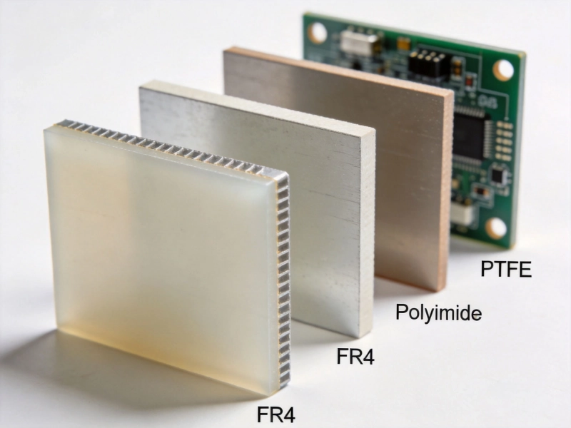
Selecting the Right Dielectric Materials for High-Performance HDI PCBsMay/28/2026
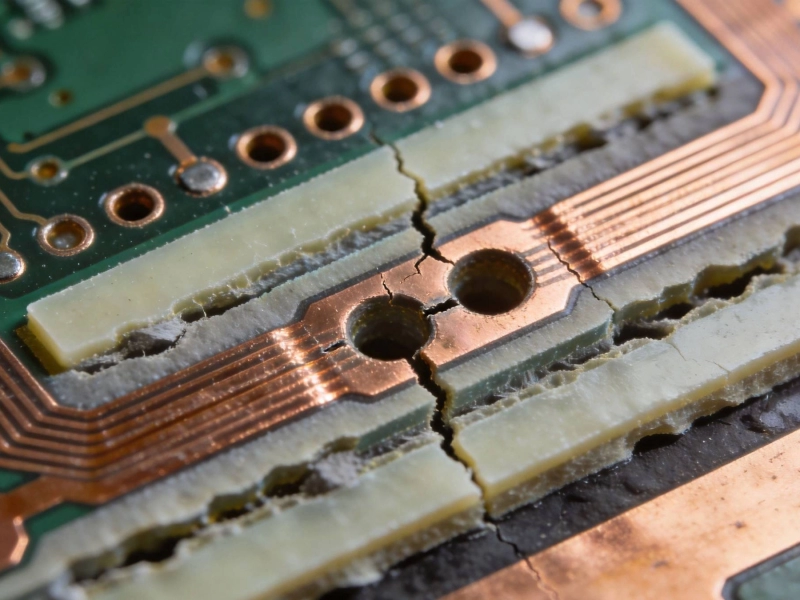
Understanding and Preventing Microvia Cracking in Thermal CyclingJune/12/2026

The Role of HDI in High-Speed Server and Data Center HardwareJuly/18/2026
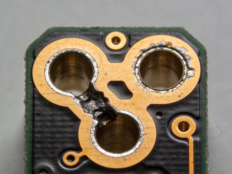
The Impact of Plating Voids on HDI Interconnect ReliabilityJuly/10/2026
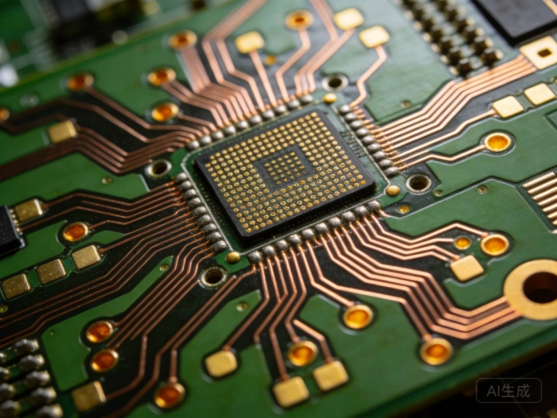
Best Practices for BGA Fanout and Routing in HDI LayoutsJuly/07/2026

HDI PCB Requirements for Mission-Critical Aerospace ApplicationsJune/30/2026