
Via-in-pad — placing a via directly within a component land pad rather than beside it — is one of the most consequential design decisions in modern PCB layout. It affects thermal performance, solder joint integrity, manufacturing cost, and long-term reliability in ways that are not always obvious from a schematic view. Done correctly, Via-in-pad dramatically improves heat extraction from power components. Done incorrectly, it creates solder defects that undermine the very reliability it was meant to enhance.
This article examines the dual nature of via-in-pad: its significant thermal benefits, the reliability risks it introduces, the manufacturing processes that mitigate those risks, and the design guidelines that help you get the thermal advantage without the reliability penalty.
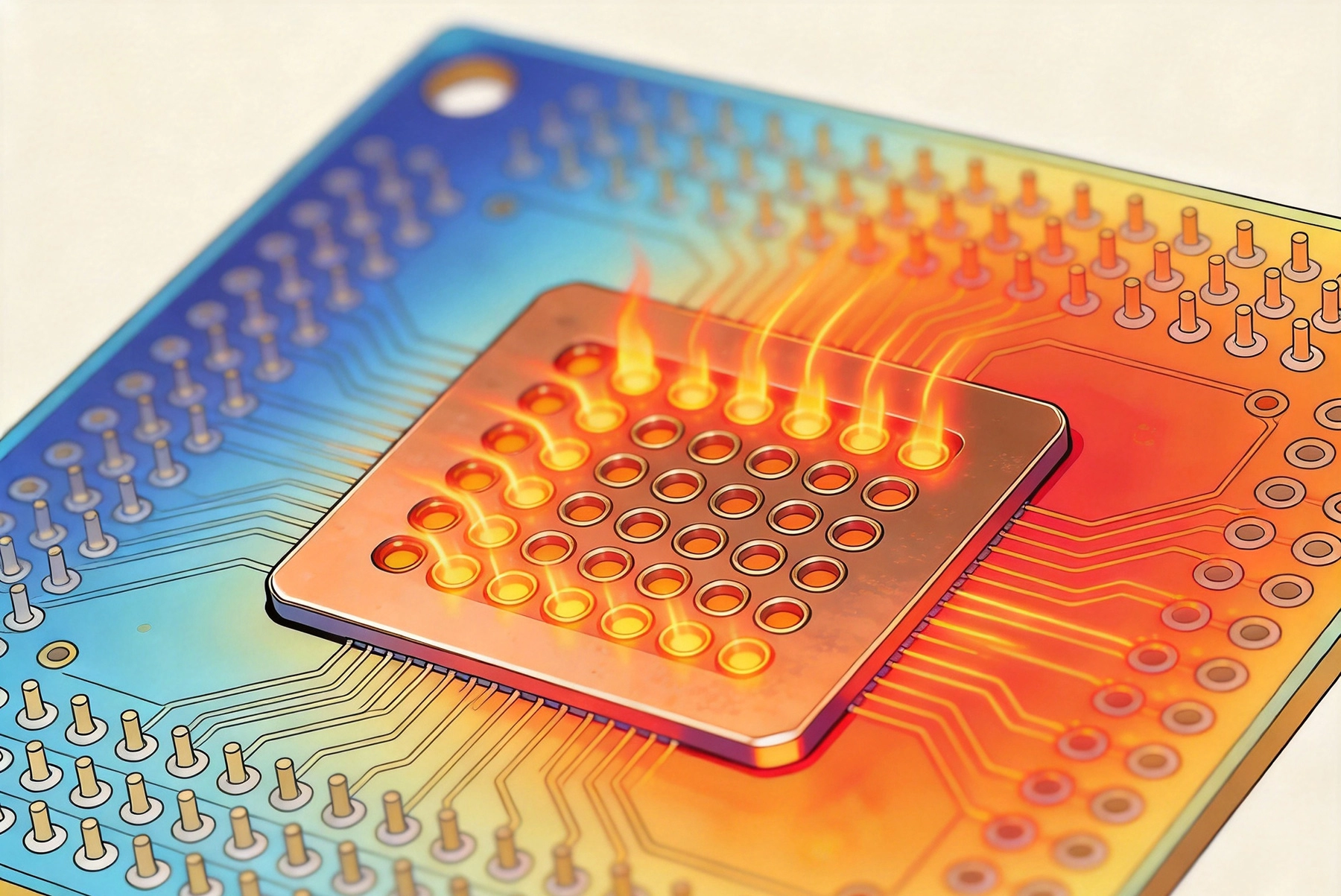
In Traditional Pcb routing, vias are placed adjacent to component pads and connected by a short trace — the "dog-bone" fanout. This approach keeps the pad surface intact for soldering but adds routing area and increases the thermal path length between the component and the internal copper plane.
Via-in-pad places the via directly within the pad. The component solder joint makes contact with the pad surface, which has a via barrel passing through it to internal layers. This eliminates the dog-bone trace, saves routing space, and — critically for power components — provides a direct, short thermal path from the component junction to internal copper planes.
The thermal advantage of via-in-pad is substantial and well-documented. By providing a direct conductive path through the PCB dielectric to internal copper planes, via-in-pad reduces the thermal resistance between the component and the heat spreading layer, lowering junction temperature for a given power dissipation.
The thermal resistance of a via-in-pad connection has two components: the via barrel (copper cylinder) and the connection to the internal plane (copper spreading). For a typical 0.3 mm diameter via with 25 µm plating in a 1.6 mm board, the via barrel thermal resistance is approximately 7-10°C/W. A 5-via array reduces this to 1.4-2.0°C/W. For a component dissipating 5 W, this via array alone can reduce the junction temperature by 7-10°C compared to a design where heat must conduct laterally through the pad and then through a dog-bone trace to a via.
For QFN thermal pads, the benefit is even more pronounced. A QFN power stage with a 3×3 mm Thermal Pad and a 5×5 array of 0.3 mm filled vias can achieve total thermal resistance (junction to ambient via the PCB path) that is 30-50 percent lower than the same component with no Thermal Vias, and 15-25 percent lower than with dog-bone vias placed around the pad perimeter.
Via-in-pad does more than just conduct heat vertically. By connecting the component pad directly to an internal copper plane, it activates the plane's lateral heat spreading capability. Copper's Thermal Conductivity (385 W/m·K) is roughly 1,000 times higher than FR4 (0.35 W/m·K). Once heat reaches the internal plane, it spreads rapidly across the plane area, effectively increasing the Heat Dissipation surface far beyond the component pad footprint.
This spreading effect means that a via-in-pad array under a small component can leverage a large internal ground or power plane as a heat sink. A 5×5 mm QFN thermal pad connected through vias to a 50×50 mm internal copper plane can achieve effective thermal performance comparable to a small external heatsink — without the cost, space, and assembly complexity of an attached heatsink.
The primary reliability risk of via-in-pad is solder wicking — the tendency of molten solder to flow into the via barrel during reflow, draining solder away from the joint between the component termination and the pad surface. This reduces the effective solder volume at the joint, creating weak or open connections.
During reflow, when the solder paste melts and becomes liquid, capillary forces draw the molten solder into any available cavity. An open via barrel is a cylindrical cavity that exerts strong capillary action on the liquid solder. The smaller the via diameter, the stronger the capillary effect (capillary pressure is inversely proportional to radius). Solder can wick down the entire via barrel, filling it from top to bottom, and leave insufficient solder on the pad surface to form a reliable joint with the component.
The severity of wicking depends on several factors:
The manufacturing solution to solder wicking is to fill the via before component placement, eliminating the cavity that draws solder away from the joint. Two primary fill methods are used in production.
Copper fill electroplates copper into the via barrel, creating a solid copper plug. After plating, the board surface is planarized (ground flat) to remove copper overburden and create a smooth, flat pad surface for soldering.
Advantages:
Limitations:
Epoxy fill uses screen-printed epoxy to fill the via barrel. Conductive epoxy contains silver or copper particles to provide electrical and thermal conductivity. Non-conductive epoxy is used when the via only needs to be plugged to prevent wicking, and electrical/thermal conductivity through the fill is not required.
Advantages:
Limitations:
Via tenting covers the via opening with solder mask, sealing the top of the via barrel. This is the lowest-cost option but has significant limitations:
Tenting is acceptable for non-critical vias where wicking risk is low (large vias with generous paste volume), but it should not be relied upon for BGA via-in-pad or QFN thermal pad vias where joint reliability is critical.
The choice of via fill method directly affects thermal performance. Here is a quantitative comparison for a typical thermal via scenario: a 0.3 mm diameter, 1.6 mm long via connecting a QFN thermal pad to an internal ground plane.
The conclusion is clear: for thermal vias under power components, copper fill provides the best thermal performance and the best reliability. Conductive epoxy is a compromise that eliminates wicking but sacrifices significant thermal performance. Non-conductive epoxy eliminates wicking but provides no thermal benefit over an unfilled via.
For applications that experience repeated temperature cycling — automotive, aerospace, industrial, and outdoor electronics — the long-term reliability of the via-in-pad connection under thermal stress is as important as its initial thermal performance.
Copper-filled vias have the best thermal cycling reliability because the fill material is metallurgically bonded to the via plating and the pad copper. There is no material interface with CTE mismatch. Under thermal cycling, the copper fill, via barrel, and pad expand and contract together, maintaining mechanical and electrical integrity through thousands of cycles.
Industry testing has demonstrated that copper-filled via-in-pad structures survive 1,000+ thermal cycles (-40°C to +125°C) with no detectable degradation in joint resistance or thermal performance. This makes copper fill the preferred choice for Class 3 and automotive applications.
Epoxy-filled vias have lower thermal cycling reliability due to CTE mismatch. Typical PCB epoxy has a CTE of 40-60 ppm/°C below Tg and 150-250 ppm/°C above Tg, while copper's CTE is 17 ppm/°C. This mismatch creates shear stress at the epoxy-copper interface with every temperature cycle.
Over hundreds or thousands of cycles, this stress can cause:
The severity depends on the cycling temperature range, the epoxy formulation, and the via geometry. For moderate cycling ranges (0°C to +85°C), conductive epoxy fill is generally reliable for 500+ cycles. For extreme ranges (-40°C to +125°C or wider), copper fill is strongly preferred.
The solder joint itself — the connection between the component termination and the pad surface — is affected by via-in-pad in several ways:
Via-in-pad with fill adds cost compared to standard vias or dog-bone routing. Understanding the cost components helps you make informed trade-offs.
For most designs with BGA or QFN components, the cost of copper-filled via-in-pad is easily justified by the improvement in first-pass yield (fewer solder defects), thermal performance (no need for external heatsinks), and long-term reliability (fewer field failures). The cost savings from avoiding rework and field returns typically exceed the incremental board cost within the first production run.
For low-power, non-safety-critical applications where the component dissipates less than 0.5 W and thermal performance is not critical, open via-in-pad without fill may be acceptable. The wicking risk is still present, but with generous solder paste volume and a reflow profile that minimizes time above liquidus, the impact may be manageable. However, you should validate this approach with first-article inspection (X-ray) to confirm that joint quality is acceptable before committing to production.
Almost always, yes — provided the vias are filled with copper. Open (unfilled) vias provide some thermal benefit through the via plating, but if solder wicks into the barrel, the thermal connection becomes inconsistent. Epoxy-filled vias improve thermal performance over no vias but underperform copper fill. The only scenario where via-in-pad does not improve thermal performance is when the internal layer the via connects to has no copper plane at that location — the via terminates in Dielectric Material and has no spreading path. Always ensure thermal vias connect to an actual copper plane.
There is no single answer — it depends on the component power dissipation, the internal plane area, the acceptable junction temperature rise, and the available pad area. As a starting point, use a via array that covers 20-30 percent of the thermal pad area, with via diameter of 0.3-0.4 mm and pitch of 0.8-1.0 mm. Then verify with Thermal Simulation or measurement that the junction temperature is within limits. Adding more vias beyond the point where the internal plane is effectively engaged yields diminishing returns.
Via-in-pad on high-frequency signal pads (RF, high-speed digital) introduces a capacitive stub — the via barrel below the pad acts as a capacitive element that can degrade Signal Integrity. For signal pads, via-in-pad should be used only when routing requires it, and the via should be back-drilled (controlled-depth drilled from the opposite side to remove the unused portion of the barrel) if the stub length would degrade signal performance. For thermal-only pads (QFN thermal pads, power tabs), capacitive stubs are not a concern because these connections are DC or low-frequency.
Yes. Microvias (laser-drilled, typically ≤ 0.15 mm diameter, connecting only 1-2 layers) have lower aspect ratios and smaller volumes than through-hole vias. This makes them easier to fill completely with copper and less prone to fill voids. However, microvias have less copper cross-section and higher thermal resistance per via than a larger through-hole via. For thermal applications where via count is limited by pad area, larger (0.3-0.5 mm) through-hole vias with copper fill generally provide better thermal performance than microvias. For BGA signal routing, microvias are preferred because they fit within fine-pitch pads and are more cost-effective to fill.
Via-in-pad is a powerful design technique that can significantly improve thermal performance and routing density — but it demands careful implementation to avoid reliability problems. The key is to match the via fill method to the application requirements: copper fill for thermal vias and critical BGA pads where maximum thermal performance and long-term reliability are required; conductive epoxy fill as a cost compromise for less demanding applications; and via tenting only for non-critical vias where wicking risk is low. Always specify via fill explicitly in your fabrication notes, verify fill quality with cross-section or X-ray, and validate the thermal performance of your via-in-pad design with measurement or simulation before committing to production. When done correctly, via-in-pad delivers the thermal and routing benefits your design needs without the reliability compromises you cannot afford.
Contact us to discuss your requirements
The Role of Thermal Vias in Dissipating Heat from HDI BoardsJune/09/2026
How to Use Thermal Simulation Software to Optimize HDI LayoutsJuly/29/2026
Thermal Management Strategies for HDI Power ModulesSeptember/11/2026
Exploring the 6 Types of HDI Structures: From Type I to Any-LayerAugust/14/2026
Selecting the Right Dielectric Materials for High-Performance HDI PCBsMay/28/2026
Effective Thermal Management Strategies for High-Density PCBsMay/28/2026
Copper Coin and Embedded Heat Sinks: Advanced Cooling for HDIJuly/08/2026

Managing Heat in High-Power HDI Applications: A Practical GuideSeptember/03/2026