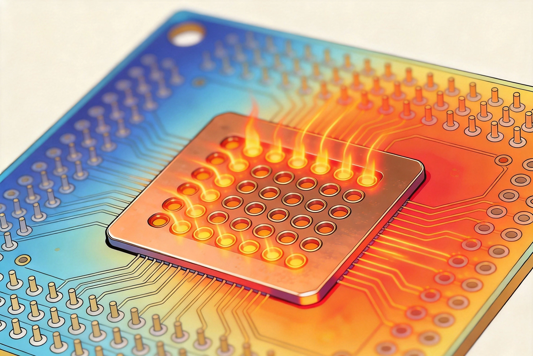
Via-in-pad — placing a via directly within a component land pad rather than beside it — is one of the most consequential design decisions in modern PCB layout. It affects thermal performance, solder joint integrity, manufacturing cost, and long-ter...