
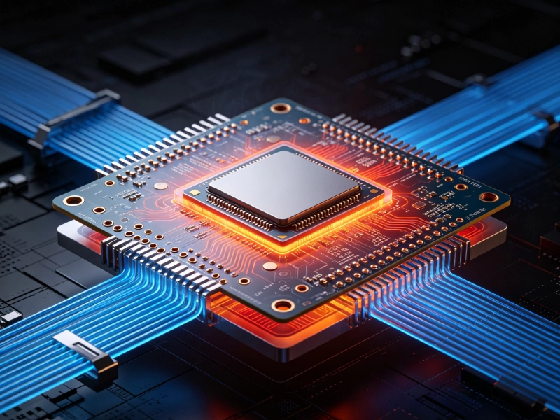
Power Electronics and High Density Interconnect (HDI) PCB technologies are increasingly combined in modern electronic systems. Server power supplies, electric vehicle chargers, industrial motor drives, and RF power amplifiers all place demanding thermal requirements on compact Hdi Boards. The challenge is acute: HDI construction concentrates components and circuitry in smaller areas, while power components generate heat that must go somewhere. If not managed effectively, this heat degrades performance, reduces reliability, and ultimately destroys the electronics.
Understanding Thermal Management for HDI power modules requires appreciating the unique challenges these designs present and the strategies available to address them. This article explores heat generation sources, thermal resistance paths, and practical design techniques for managing temperatures in dense power electronic assemblies.
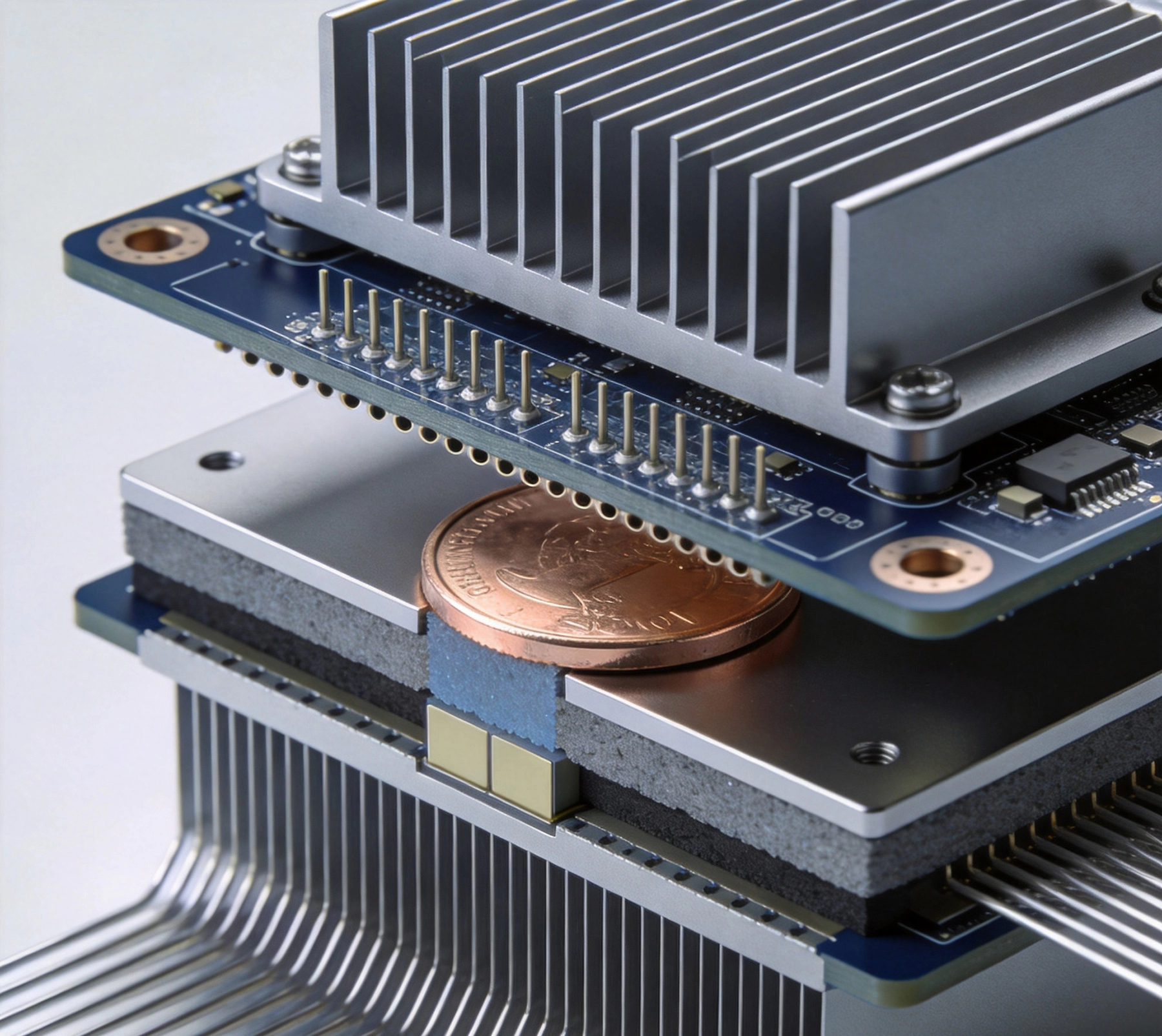
HDI technologies enable Miniaturization by using Microvias, Blind Vias, and finer trace geometries to pack more functionality into smaller areas. While excellent for signal routing density, this same concentration creates thermal challenges. Power components generate heat, and in dense HDI assemblies, that heat must flow through increasingly constrained thermal paths.
Thermal runaway is a particular risk in dense power modules. As temperature increases, component parameters shift, often increasing power dissipation, which further raises temperature. Without adequate thermal paths to remove heat, this positive feedback loop can rapidly destroy components or cause safety failures.
The Thermal Conductivity of Pcb Materials is typically very low, around 0.3 to 0.5 W/mK for standard FR-4. This makes the PCB itself a relatively poor heat conductor compared to metals. Getting heat out of the board and into a Thermal Management structure requires deliberate design.
All conductors carrying current dissipate power according to the formula P = I squared times R. For power semiconductors conducting substantial currents, conduction losses represent significant heat generation. MOSFETs and diodes in power conversion applications dissipate watts to tens of watts in a compact area, creating localized hot spots.
The challenge is that the most efficient semiconductors, those with the lowest on-resistance, are often the smallest packages. This concentration of dissipation in a small area creates steep thermal gradients and demands efficient heat spreading before the heat can be conducted away.
In switching power supplies and motor drives, transistors transition between on and off states thousands or millions of times per second. During these transitions, voltage and current overlap momentarily, creating switching losses. At high frequencies, switching losses can dominate the thermal budget.
Switching losses depend on the speed of transitions and the frequency of operation. Faster transitions reduce switching loss but create electromagnetic interference challenges. Higher frequencies allow smaller magnetics but increase switching losses. Thermal management must account for both conduction and switching contributions to total dissipation.
Inductors and transformers in power modules generate heat from copper losses in windings and core losses in magnetic materials. These losses increase with frequency and current. Dense power modules often use planar magnetics with copper traces as windings, integrating them into the PCB structure for compactness.
Planar magnetics present particular thermal challenges because they are embedded within the PCB stackup. Heat generated in the magnetic core must conduct through surrounding dielectric layers before reaching any thermal management structure. Careful material selection and thermal via placement help address these challenges.
Heat flows from hot regions to cooler regions following the path of least thermal resistance. Understanding these paths is essential for effective thermal management. The thermal resistance of each element in the heat flow path determines how efficiently heat moves and where temperature drops occur.
For semiconductor devices, the first thermal resistance in the path is from the semiconductor junction to the package case. This resistance is determined by the device construction and is specified by the manufacturer. Lower junction-to-case resistance indicates better internal thermal paths.
When selecting power semiconductors, compare thermal resistance specifications carefully. A device with lower on-resistance may actually have higher junction-to-case resistance, requiring better external thermal management to achieve the same junction temperature.
At every interface between materials, thermal resistance occurs due to imperfect contact and different thermal conductivities. The interface between a component package and a heatsink, or between a PCB and a Thermal Pad, adds resistance to the heat flow path.
Thermal interface materials (TIM) reduce interface resistance by filling air gaps and providing high-conductivity paths across imperfect contacts. TIM selection affects overall Thermal Performance significantly, particularly in applications where component packages have high heat flux.
Heat spreading through a material occurs in two or three dimensions, creating spreading resistance. When heat from a small source flows into a larger area, the temperature drop across the spreading path depends on the geometry and Thermal Conductivity of the material.
In HDI power modules, copper planes serve as heat spreaders. The copper in power and ground planes distributes heat from localized sources to larger areas, reducing temperature rise. Adequate copper thickness and area improve spreading performance.
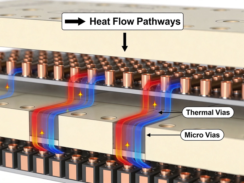
Thermal Vias provide conductive heat paths through the PCB from hot components to other layers or to thermal structures on opposite sides of the board. Properly designed Thermal Vias dramatically improve heat removal from surface-mounted power components.
Thermal via effectiveness depends on via diameter, spacing, plating thickness, and the thermal conductivity of any fill material. Larger vias with heavier plating conduct more heat. Tighter spacing reduces spreading resistance between vias.
Standard thermal via designs use vias of 10 to 20 mils diameter, with spacing of 20 to 40 mils. For extreme thermal demands, larger thermal vias with heavy plating and solder fill can achieve thermal conductivities approaching solid copper. The tradeoff is that larger vias consume more board area and may affect routing density.
The placement of thermal vias relative to heat sources significantly affects Thermal Performance. Vias should be placed directly under hot components, with the array sized to match the component footprint. Thermally conductive pads on component pads, called thermal pads, connect the component to the via array.
Thermal Pad design balances thermal performance against manufacturability. Larger thermal pads improve thermal performance but may conflict with routing or create solder paste issues. Many manufacturers have standard thermal pad and via array designs optimized for common component packages.
Hdi Technology enables blind and Buried Vias that connect specific layers without penetrating the entire board. Blind thermal vias connecting surface components directly to internal heat spreading layers reduce thermal resistance compared to through-vias that must traverse the entire stackup.
Buried thermal vias connecting internal layers enable heat spreading between internal planes. These structures are more expensive to manufacture but provide thermal paths not achievable with standard through-via technology.
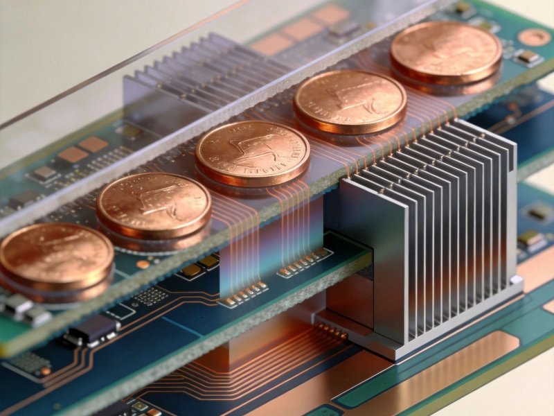
Copper coin inserts place solid copper slugs within the PCB stackup directly beneath heat sources. These coins provide very high thermal conductivity paths from the component attachment surface to thermal vias or mounting points on the opposite side of the board.
The copper coin technique is particularly effective for high-power modules where standard thermal vias cannot provide sufficient heat removal. The thermal conductivity of solid copper, around 400 W/mK, vastly exceeds that of plated vias or dielectric materials.
Manufacturing copper coin structures requires specialized processes where the coin is placed during lamination and the stackup is built around it. Not all manufacturers support this technique, and those that do typically have minimum requirements for coin size and placement.
Building on the copper coin concept, embedded coin technology integrates solid metal heat spreaders at specific locations within the PCB stackup. These spreaders can be shaped to cover specific component footprints or to span multiple heat sources, distributing heat over larger areas.
Embedded coins connect to component attachment surfaces through thermal vias or direct metallization. The thermal path from the component to the embedded coin can be made extremely low resistance with proper design, enabling high-power-density modules that would not be feasible with standard Pcb Materials.
Some manufacturers offer direct metal bonding processes where copper is bonded directly to ceramic substrates or metal core materials. This technique eliminates the thermal resistance of dielectric adhesive layers, creating very efficient thermal paths.
Direct bonded copper (DBC) and active metal brazed (AMB) substrates use ceramic dielectrics with direct copper bonding for superior thermal performance. These substrates are common in high-power modules but add significant cost compared to standard PCB materials.
Heatsinks attached to PCBs increase the effective surface area for convection and radiation cooling. For HDI power modules, heatsinks can be attached to the component side, the back side, or both sides of the board, depending on thermal requirements and packaging constraints.
Clip-mounted heatsinks allow field replacement and testing before permanent attachment. Adhesive-mounted heatsinks provide lower profile solutions but cannot be easily removed. Soldered heatsinks provide the lowest thermal resistance but prevent component replacement and require specialized assembly processes.
The interface between the heatsink and PCB represents a significant thermal resistance in the heat flow path. Selecting appropriate thermal interface materials and ensuring proper application are critical to heatsink performance.
Thermal interface materials range from thermal greases with very low resistance to compliant thermal pads that are easier to apply. Phase change materials that liquefy when heated provide good performance with forgiving application tolerances.
Bond line thickness affects thermal resistance. Thinner bond lines reduce resistance but require more precise mounting. Void-free application is important because air gaps dramatically increase thermal resistance. Many manufacturers specify application pressure and methods to achieve consistent bond lines.
For extreme thermal demands, active cooling using fans or liquid cooling cold plates may be necessary. These approaches dramatically increase heat removal capacity but add complexity, cost, and reliability considerations.
Forced air cooling using fans dramatically improves convection coefficients. The airflow path, fan placement, and airflow impedance of surrounding structures affect cooling effectiveness. Computational fluid dynamics simulation helps optimize airflow design for active cooling systems.
Liquid cooling using cold plates offers the highest heat removal capacity. Cold plate integration in HDI power modules requires sealed fluid connections, careful attention to leak prevention, and sometimes specialized PCB constructions with embedded cooling channels.
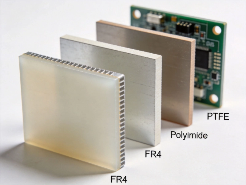
Standard FR-4 materials have thermal conductivity around 0.3 W/mK, making them relatively poor heat conductors. Alternative substrates offer significantly higher thermal conductivity at various cost and performance points.
Metal core substrates use aluminum or copper base materials with thermal conductivities of 1 to 10 W/mK or higher. These materials spread heat from hot components over larger areas before conducting to attachment points or heatsinks. Metal core PCBs are common in LED lighting and power conversion applications.
Ceramic-filled substrates offer intermediate thermal conductivity with good electrical performance. Alumina (Al2O3) and aluminum nitride (AlN) substrates provide thermal conductivities from 20 to 170 W/mK depending on material. These substrates are more expensive than organic materials but enable high-power-density designs.
Even within standard FR-4 families, thermal conductivity varies. Some high-Tg materials offer improved thermal conductivity while maintaining the processing advantages of standard FR-4. These materials provide marginal but sometimes significant improvement in thermal spreading.
Thermally conductive prepregs use ceramic or metal oxide fillers to increase thermal conductivity. These materials provide improved thermal paths through the PCB stackup while maintaining good electrical properties. Processing requirements differ from standard prepregs, and manufacturer guidance should be followed for optimal results.
Attaching a metal backplane to the PCB dramatically improves thermal spreading and provides a conduction path to mounting surfaces. The metal backplane can be attached using thermal adhesive, mechanical fasteners with thermal washers, or solder bonding for lowest thermal resistance.
The choice of attachment method affects both thermal resistance and serviceability. Soldered attachments provide the best thermal performance but prevent component rework on the primary side. Adhesive attachment provides good thermal performance with field serviceability, though the adhesive adds thermal resistance.
The small via diameters in HDI construction limit thermal via conductivity compared to standard through-vias. The thermal conductivity of a Microvia depends on its plating thickness, which may be thinner than standard vias due to plating uniformity challenges in small features.
For thermal-critical applications, specifying heavier plating on thermal Microvias helps compensate for reduced diameter. Some manufacturers offer thermal Via Filling processes that pack the via with thermally conductive material for improved performance.
The PCB stackup in HDI designs affects thermal paths significantly. Placing power and ground planes near the surface with hot components improves heat spreading. Using thinner dielectrics between the component layer and thermal planes reduces thermal resistance.
For designs with embedded coins or thermal spreaders, the stackup must be optimized around the embedded structure. This requires close coordination with the manufacturer during the design phase to ensure the stackup supports both thermal and electrical requirements.
In dense HDI assemblies, component placement affects both thermal performance and manufacturing efficiency. Placing high-power components near board edges or thermal interface areas allows heat to flow to heatsinks or mounting surfaces without crossing sensitive signal routing.
Spreading heat sources across the board rather than concentrating them reduces local temperature peaks. This approach may require longer traces or additional layers but often enables adequate thermal management without exotic thermal solutions.
Computational Thermal Simulation has become essential for HDI power module design. Finite element analysis (FEA) tools predict temperature distributions based on geometry, materials, power dissipation, and boundary conditions. These predictions guide design optimization before physical prototypes are built.
Most PCB Thermal Simulation tools accept power dissipation inputs from circuit simulation or measurement, material thermal properties from vendor data, and boundary conditions from expected operating environments. Results guide thermal pad design, via placement, and material selection.
Simulation predictions should be validated against physical measurements. Thermocouples, thermal imaging cameras, and resistance thermometry provide temperature data for model correlation. Discrepancies between simulation and measurement guide model refinement.
Thermal test boards with instrumented components and embedded temperature sensors validate designs before production release. These boards often include multiple design variations to explore thermal optimization options efficiently.
Thermal stress testing exposes HDI power modules to elevated temperatures to identify failure mechanisms related to thermal fatigue. Temperature cycling, high-temperature operating life tests, and power temperature cycling accelerate failure mechanisms to compress validation timelines.
Failure analysis of tested units reveals failure modes and guides design improvements. Common thermal failure modes in HDI power modules include solder joint fatigue, via barrel cracking, delamination, and component degradation. Each failure mode has specific design and manufacturing remedies.
Thermal management for HDI power modules benefits from early manufacturer engagement. Discussing thermal requirements during the stackup design phase allows optimization of materials and structures for thermal performance. Waiting until the layout is complete may limit thermal solutions to expensive additions rather than integrated optimizations.
Manufacturers experienced with thermal-critical designs can suggest stackup options, thermal via specifications, and interface options based on their process capabilities. This expertise is most accessible when incorporated into the design process early.
For challenging thermal designs, thermal test vehicles isolate thermal design variables for systematic evaluation. These test vehicles use standardized component footprints and thermal structures to compare materials, via designs, and interface options under controlled conditions.
Thermal test vehicle results provide data for simulation correlation and design selection. The investment in test vehicle fabrication and testing often returns through reduced prototype iterations and improved first-pass design success.
Thermal management in HDI power modules presents unique challenges that require deliberate design attention. The concentration of power components in dense HDI assemblies demands efficient thermal paths from heat sources to heat sinks or mounting surfaces. Understanding heat generation mechanisms, thermal resistance paths, and available mitigation strategies enables effective thermal design.
The thermal management toolkit for HDI power modules includes thermal vias, copper coins, embedded heat spreaders, alternative substrates, heatsink integration, and active cooling. Each solution offers tradeoffs among thermal performance, cost, manufacturing complexity, and serviceability. The appropriate solution depends on the specific thermal requirements, volume, and application constraints of each design.
Early attention to thermal requirements, simulation-based design optimization, and manufacturer collaboration on thermal structures enable successful HDI power module development. As power density requirements continue to increase, thermal management will remain a critical discipline for successful high-density Power Electronics.
There is no single most effective technique. The best approach depends on power density, available board area, thermal environment, and cost constraints. For moderate power densities, thermal vias with copper spreading planes often suffice. For extreme power densities, copper coins or embedded heat spreaders combined with heatsink attachment may be necessary. Often a combination of techniques provides the best overall solution.
Thermal via count depends on the heat flux from the component, the allowable temperature rise, and the thermal resistance of each via. Simulation tools predict performance for different via counts, and thermal test vehicles validate predictions. Manufacturer guidelines based on component packages provide starting points for typical applications.
Solid copper has thermal conductivity around 400 W/mK. A typical thermal via with 1 mil plating might have effective thermal conductivity of 50 to 100 W/mK depending on geometry. A copper coin provides thermal conductivity approaching solid copper and can be made much larger than vias, providing substantially lower thermal resistance for high-power applications.
Thermal vias under power components provide clear thermal benefit. Thermal vias under other components may provide marginal benefit or may complicate routing without meaningful thermal improvement. Focus thermal via investment on components that dissipate significant heat. Signal and passive components typically benefit more from good grounding and decoupling than from dedicated thermal vias.
HDI construction can both help and hinder thermal performance. Benefits include the ability to place thermal planes close to the component surface and the integration of buried thermal vias. Challenges include smaller via diameters limiting thermal via conductivity and more complex stackups requiring careful thermal path design. Overall, HDI can achieve excellent thermal performance with proper design but requires more deliberate attention to thermal paths.
The Impact of Via-in-Pad on Thermal Performance and ReliabilitySeptember/26/2026
Effective Thermal Management Strategies for High-Density PCBsMay/28/2026
How to Use Thermal Simulation Software to Optimize HDI LayoutsJuly/29/2026
The Role of Thermal Vias in Dissipating Heat from HDI BoardsJune/09/2026
Managing Heat in High-Power HDI Applications: A Practical GuideSeptember/03/2026
Copper Coin and Embedded Heat Sinks: Advanced Cooling for HDIJuly/08/2026
Selecting the Right Dielectric Materials for High-Performance HDI PCBsMay/28/2026
Exploring the 6 Types of HDI Structures: From Type I to Any-LayerAugust/14/2026