Open Nav

High-density Interconnect (HDI) printed circuit boards represent the cutting edge of Pcb Manufacturing, enabling finer trace widths, smaller vias, and higher component densities than conventional multilayer boards. But with this complexity comes a critical question for every engineer and procurement professional: how long does it actually take to manufacture custom Hdi Boards?
The short answer is that lead times for custom Hdi Boards typically range from 5 to 25+ business days, depending on board complexity, layer count, via structure, and the manufacturer's production capacity. However, the full picture is far more nuanced. This article breaks down the factors that drive HDI lead times, explains each stage of the manufacturing process, and provides practical guidance for planning your HDI projects.
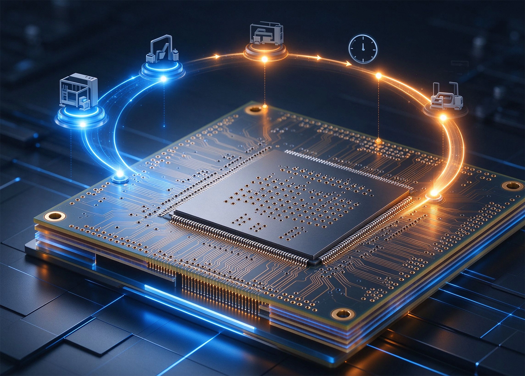
Before diving into the details, here is a quick reference for typical Hdi Manufacturing lead times by complexity tier:
| Complexity Tier | Typical Lead Time | Example Characteristics |
|---|---|---|
| Simple HDI (1-step HDI) | 5–10 business days | 1–2 HDI layers, Microvias on outer layers only, 4–6 total layers |
| Moderate HDI (2-step HDI) | 10–15 business days | Stacked or staggered Microvias, 6–10 total layers, Via-in-pad |
| Complex HDI (3+ step HDI) | 15–25+ business days | Any-layer Hdi, 10+ layers, stacked microvias, filled vias, fine-pitch BGA |
| Ultra-Complex / Substrate-Like | 25–40+ business days | SLP (substrate-like PCB), mSAP process, ≤20 μm trace/space, 12+ layers |
These are standard lead times from order confirmation to shipment. Expedited (rush) options may reduce these by 30–50% at a significant cost premium, typically 50–200% above standard pricing.
To understand HDI lead times, it helps to compare the manufacturing flow of a standard Multilayer Pcb versus an HDI board.
A standard 4–8 layer board can often be completed in 3–7 business days because the process is largely linear and uses well-established, high-throughput equipment.
The key difference is that each HDI step adds an entire lamination cycle, which includes laser drilling, desmear, via filling, plating, and pressing. A 3-step HDI board may go through the lamination press four or more times, compared to once for a standard multilayer board. Each cycle adds 1–3 business days to the lead time.
This is the single largest determinant of HDI lead time. Each "step" corresponds to one additional Sequential Lamination cycle:
Rule of thumb: each additional HDI step adds approximately 3–5 business days to the lead time.
While HDI step count is the primary driver, total layer count also matters. A 12-layer any-layer HDI board will take significantly longer than a 6-layer 1-step HDI board, simply because there are more layers to image, align, and laminate.
Finer features require more careful processing:
Some surface finishes add processing time:
Even with identical board designs, lead times can vary significantly between manufacturers based on:
Here is a typical time allocation for a moderate-complexity 2-step HDI board (8 layers, stacked microvias, via-in-pad, ENIG):
| Stage | Duration | Notes |
|---|---|---|
| Engineering review / CAM preparation | 1–2 days | DFM check, impedance modeling, panelization, tooling design |
| Inner layer fabrication (cores 1–2) | 2–3 days | Imaging, etching, AOI for first set of cores |
| First lamination cycle + laser drilling | 2–3 days | Layup, press, laser drill microvias, desmear |
| Via filling and plating (step 1) | 1–2 days | Epoxy fill or copper fill, surface planarization |
| Second lamination cycle + laser drilling | 2–3 days | Second layup, press, laser drill outer microvias |
| Via filling and plating (step 2) | 1–2 days | Second round of via fill if needed |
| Final lamination and outer layer processing | 2–3 days | Final press, outer imaging, pattern plating, etching |
| AOI, solder mask, surface finish | 2–3 days | Final imaging, LPI application, ENIG plating |
| Profiling, electrical testing, QA | 1–2 days | Routing/scoring, flying probe or fixture test, final inspection |
| Total (typical) | 14–23 days | Overlaps between stages can reduce total calendar time |
Note: Many of these stages can overlap in a well-run factory (e.g., inner layer fabrication of one set of cores while another set is being laminated), so the actual calendar time is often less than the sum of individual stages.
The most effective way to reduce lead time is to design your board with manufacturing efficiency in mind:
Engage your PCB supplier during the design phase, not after layout is complete. A good manufacturer can:
Most HDI manufacturers offer expedited options:
Be aware that expedited orders increase the risk of quality issues because there is less time for in-process inspection and rework.
Panelizing multiple boards into a single production panel can reduce per-unit lead time by amortizing setup time across more units. However, complex panelization (odd shapes, mixed designs) can add engineering time. Work with your manufacturer to find the optimal panelization approach.
HDI boards require more extensive CAM engineering than standard PCBs. Impedance modeling, microvia aspect ratio verification, and stackup optimization can take 1–3 days before production even begins. Factor this into your schedule.
Specialty laminates (high-frequency materials like Rogers RO4000 series, Low-loss Materials like Megtron 6, or high-Tg materials) may not be in stock and can add 3–10 days for procurement. Always confirm material availability before placing an order.
HDI boards have less margin for error. If a batch fails electrical testing or Aoi Inspection, rework may not be possible, and a respin can add a full lead time cycle. Invest in thorough DFM review and prototype validation before committing to production volumes.
If your manufacturer is overseas, factor in 3–7 days for international shipping (DHL/FedEx) or 2–4 weeks for sea freight. Customs clearance can add unpredictable delays, especially for boards with certain materials or finishes.
Here is a practical framework for planning HDI projects:
Total prototype timeline: 4–8 weeks for 1-step HDI, 6–12 weeks for complex HDI.
Total production timeline: 3–6 weeks from order to delivery for most HDI projects.
HDI board manufacturing is inherently more time-intensive than standard PCB production due to the sequential lamination cycles, laser drilling, via filling, and additional inspection steps required. A realistic expectation is 5–10 business days for simple 1-step HDI, 10–15 days for moderate 2-step HDI, and 15–25+ days for complex any-layer HDI designs.
Key strategies for managing HDI lead times include:
By understanding the manufacturing process and the factors that drive lead times, you can plan your HDI projects more effectively, set realistic expectations with stakeholders, and avoid costly delays in your product development timeline.
Understanding Sequential Lamination in Multi-Step HDI BoardsJuly/03/2026
The Challenge of Plating and Filling Microvias in HDI ProductionJuly/26/2026
Overcoming Common Manufacturing Defects in High-Density InterconnectsSeptember/21/2026
How Manufacturers Achieve High Precision Alignment in 10+ Layer HDI BoardsAugust/15/2026
Precision in HDI FabricationJune/04/2026
Critical Quality Checkpoints in the HDI Production LineJuly/13/2026
HDI PCB Cost Guide: What Factors Drive the Price Up?June/16/2026
Designing Rugged HDI Boards for Harsh Industrial EnvironmentsJuly/20/2026