
High Density Interconnect (HDI) boards with 10 or more layers represent the cutting edge of printed circuit board technology. These complex multilayer structures enable high-performance electronics for applications ranging from smartphones and servers to automotive systems and aerospace equipment. However, the precision required to align multiple layers with Microvias and fine features presents extraordinary manufacturing challenges. Achieving sub-25 micron alignment accuracy across ten or more stacked layers demands specialized equipment, sophisticated processes, and meticulous Quality Control.
As component densities increase and via sizes shrink below 100 microns, the margin for error becomes vanishingly small. A misalignment of just 25 microns can cause via failures, open circuits, or electrical shorts in 10+ layer Hdi Boards. This article explores the advanced manufacturing techniques and technologies that enable high-precision layer alignment, from initial imaging through final lamination, and examines how manufacturers ensure reliability in these demanding structures.
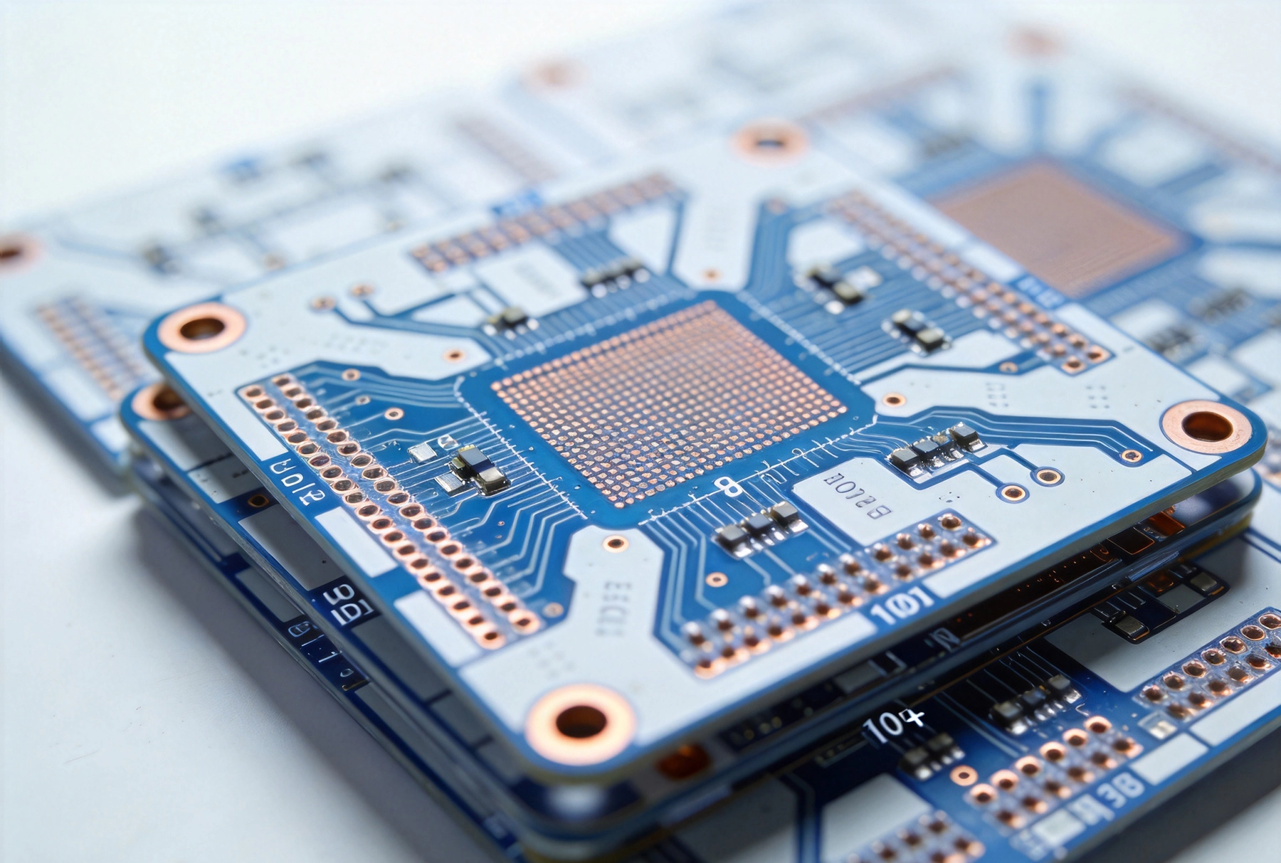
The fundamental challenge in multilayer PCB Fabrication lies in managing cumulative tolerances. With each additional layer, potential alignment errors accumulate:
In a 10-layer board, a 10-micron error per layer could accumulate to 100 microns of misalignment—completely unacceptable for modern HDI designs.
Hdi Technology introduces additional alignment challenges:
These requirements push the limits of conventional manufacturing capabilities, necessitating specialized approaches.
High-precision alignment begins with sophisticated registration mark systems:
Registration marks typically use high-contrast copper patterns visible throughout the manufacturing process.
Traditional single-point registration cannot achieve HDI precision requirements. Advanced systems use:
Multi-point registration compensates for material stress, thermal expansion, and process-induced distortions.
Traditional phototool-based imaging introduces alignment errors through:
Laser Direct Imaging eliminates these issues by directly exposing photoresist with computer-controlled laser beams.
Modern LDI systems provide exceptional alignment precision:
LDI enables tight alignment without the physical artifacts that limit contact imaging precision.
10+ layer Hdi Boards typically use Sequential Lamination rather than one-shot pressing:
This approach provides multiple alignment checkpoints and correction opportunities.
Blind and Buried Vias require special alignment techniques:
Laser Drilling systems with vision guidance can achieve ±15 micron positioning accuracy.
Material choice significantly impacts alignment capability:
Advanced materials like polyimide offer superior dimensional stability compared to standard FR-4.
Material moisture content affects dimensional stability:
Modern drilling equipment provides exceptional positional accuracy:
High-end drilling systems achieve ±12.5 micron positional accuracy, essential for 10+ layer HDI boards.
CO2 and UV laser systems create microvias with precision:
Continuous measurement ensures alignment throughout manufacturing:
Industry standards define alignment requirements:
For 10+ layer HDI boards, manufacturers typically target ±25 micron or better layer-to-layer alignment.
Pcb Materials expand and contract during processing:
Manufacturers develop compensation factors based on empirical data to counteract these effects.
Various manufacturing steps cause predictable distortions:
Understanding these effects allows pre-compensation in design and processing.
Microscopic examination provides definitive alignment verification:
Functional testing confirms alignment effectiveness:
Artificial intelligence enhances alignment control:
New technologies push alignment precision further:
Evaluating potential HDI manufacturers:
Key performance indicators for Hdi Manufacturing:
Achieving high precision alignment in 10+ layer HDI boards represents one of the most demanding challenges in printed circuit board manufacturing. Success requires integrating multiple advanced technologies—laser direct imaging, precision drilling systems, Sequential Lamination processes, and sophisticated Quality Control—into a cohesive manufacturing workflow.
The manufacturers who excel in this domain combine state-of-the-art equipment with deep process knowledge accumulated through years of experience. They understand that precision alignment is not achieved through a single technology but through careful management of every variable that affects dimensional accuracy—from material selection through final inspection.
As electronic products continue pushing toward higher densities, smaller components, and more layers, the alignment challenges will only increase. The manufacturers who have mastered precision alignment for today's 10+ layer boards will be best positioned to meet the even more demanding requirements of future generations of Hdi Technology.
Our facility specializes in 10+ layer HDI boards with microvias and tight registration requirements. With advanced LDI systems, precision drilling, and rigorous quality control, we deliver the High-density Interconnect solutions your advanced products demand. Contact us to discuss your Hdi Manufacturing needs.
Leading manufacturers achieve ±12.5 to ±25 micron layer-to-layer alignment for complex HDI structures. The exact capability depends on specific design features, material choices, and the manufacturer's equipment and processes.
LDI eliminates the dimensional instability of film phototools, provides automatic registration compensation, and enables ±12.5 micron positioning accuracy. It also allows for panel distortion mapping and correction that contact imaging cannot achieve.
Internal alignment is verified through X-ray Inspection, cross-sectional microscopic analysis of sample sections, and electrical testing that confirms via connections. In-process AOI systems also check alignment during manufacturing.
Primary causes include material thermal expansion, moisture absorption, phototool dimensional instability, mechanical positioning limitations, process-induced stresses from etching and plating, and lamination material flow variations.
Once layers are laminated together, internal alignment errors cannot be corrected. External features can sometimes be adjusted through selective routing, but internal misalignment typically results in scrap or limited functionality. Prevention through precise process control is essential.
Critical Quality Checkpoints in the HDI Production LineJuly/13/2026
The Challenge of Plating and Filling Microvias in HDI ProductionJuly/26/2026
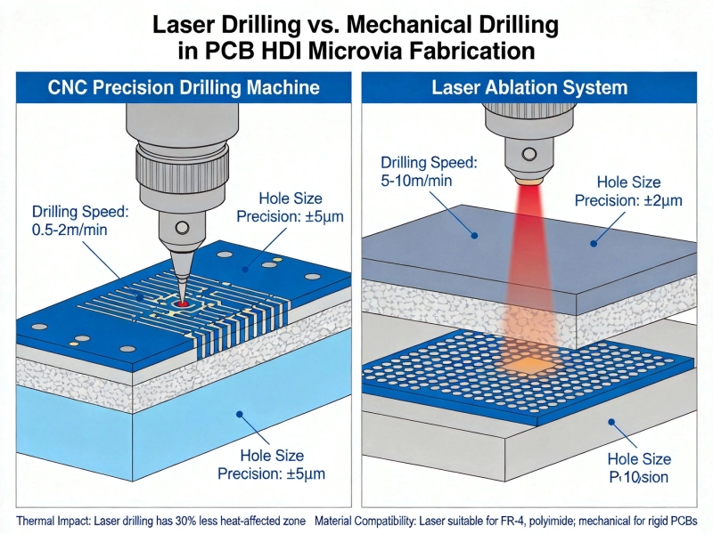
Precision in HDI FabricationJune/04/2026
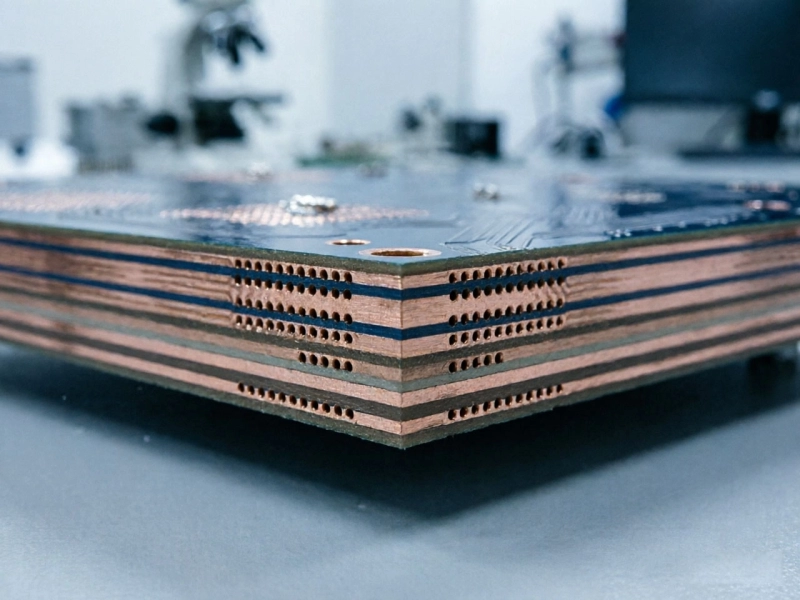
Understanding Sequential Lamination in Multi-Step HDI BoardsJuly/03/2026
What is the Lead Time for Manufacturing Custom HDI Boards?October/12/2026
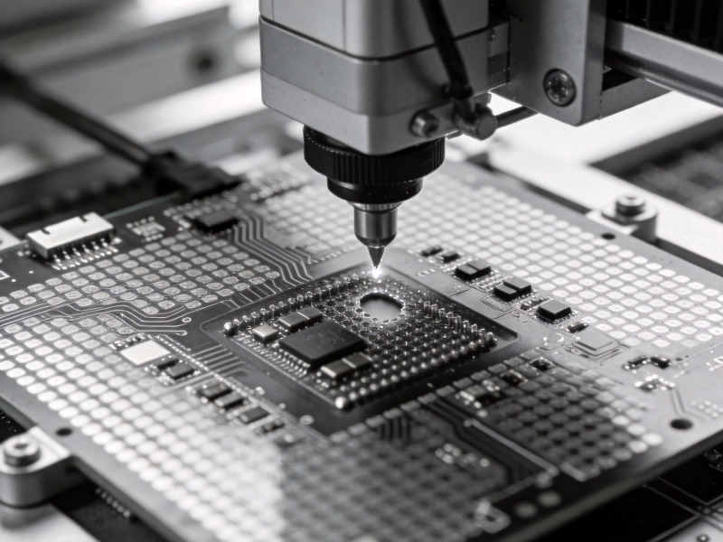
Overcoming Common Manufacturing Defects in High-Density InterconnectsSeptember/21/2026
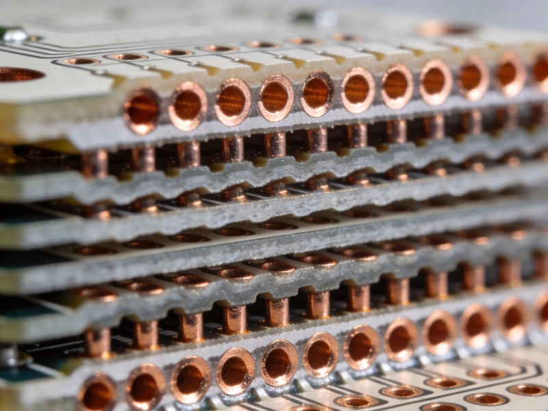
The Art of Microvia Placement: Staggered vs. Stacked ViasSeptember/24/2026
Using HDI Technology in Solar Inverters and ConvertersOctober/14/2026