Open Nav

High Density Interconnect boards deliver remarkable functionality in compact packages—fine-pitch components, blind and Buried Vias, and dense routing that would be impossible in standard multilayer constructions. This capability comes with complexity that standard consumer designs can absorb but industrial applications cannot. When Hdi Boards encounter thermal cycling, vibration, moisture, and chemical exposure, the same features that make them dense make them vulnerable.
I've worked with HDI designs ranging from medical imaging equipment to mining sensor systems. The challenges overlap substantially—size constraints demand density, but reliability demands ruggedization that standard HDI processes don't provide automatically. The solutions aren't intuitive and sometimes require tradeoffs that feel wrong until you understand the failure mechanisms they're preventing.
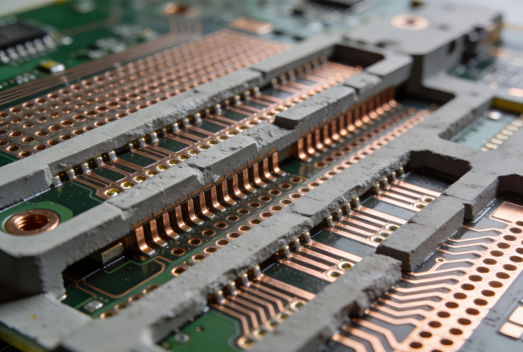
Standard multilayer boards have relatively thick dielectrics between layers, generous pad sizes, and vias that are easy to inspect and repair. HDI stacks everything tighter—thinner prepregs, smaller capture pads for Microvias, and structures that are invisible to standard inspection. The tolerances are tighter and the consequences of deviation are greater.
Microvias are the most vulnerable HDI feature in harsh environments. A laser-drilled Microvia with 0.15mm diameter and 0.20mm capture pad sits at the edge of manufacturing capability. The thermal expansion mismatch between copper barrel and dielectric creates cyclic stress with every temperature change. In a consumer product with mild thermal cycling, the stress margin suffices. In an industrial environment with wide temperature swings, the same Microvia may fail within a few thousand cycles.
The thin dielectrics in HDI stacks provide less thermal buffer than standard constructions. When components generate heat, the thin dielectric layers conduct it more readily—which sounds good until you realize this means less material available to absorb thermal shock. The temperature rise and fall at the active layer happens faster, creating steeper thermal gradients that stress the materials more aggressively.
Sequential Lamination—the process of building up HDI layers one or two at a time—creates interfaces between build-up sections. Each interface is a potential delamination site under thermal or mechanical stress. The more build-up sections, the more interfaces, the higher the cumulative delamination risk.
For industrial HDI designs, minimizing sequential build-up count pays reliability dividends. A single-step HDI build with two additional layers adds only one new interface. A three-step build with five or six layers adds three interfaces, each requiring careful process control to maintain integrity. When your application can tolerate it, reducing the HDI complexity eliminates failure modes that more complex builds cannot fully mitigate.
Core-based HDI constructions embed thin cores between outer layers, achieving density through the core's built-in microvia structure rather than through sequential build-up. The approach creates fewer interfaces than pure sequential build-up and often produces more uniform mechanical properties. The tradeoff is reduced routing flexibility compared to fully sequential constructions, but the reliability improvement often justifies the constraint.
Any-layer Hdi—sometimes called ALH—allows microvias on any layer with any-to-any connectivity. The capability is remarkable for routing density but requires six or more metal layers with dozens of sequential processing steps. Each additional step adds process variability. Any-layer Hdi in industrial applications requires explicit reliability qualification to confirm that the manufacturing process can produce consistent boards that survive the expected environmental conditions.
Thermal cycling fatigue in microvias follows predictable patterns that good design can mitigate. The copper barrel expands and contracts with temperature changes, but its expansion is constrained by the Dielectric Material surrounding it. This constraint creates cyclic shear stress at the barrel-to-pad interface. Over enough cycles, the stress produces cracks that propagate from high-stress locations—typically the barrel corners—until the connection opens.
Microvia geometry determines stress concentration magnitude. Taller, narrower vias experience higher stress than shorter, wider ones. Stacked Microvias—where one microvia lands on another—concentrate stress at both the top and bottom interfaces, making them more vulnerable than Via-in-pad constructions where the microvia lands on a solid plane. For harsh environment applications, prefer staggered microvia constructions where each microvia lands on a plane or solid copper rather than on another microvia.
Copper barrel thickness matters substantially. Standard HDI microvia plating provides 15-25 microns of copper—thin enough to be flexible but also thin enough to fatigue quickly under thermal cycling. Heavy copper microvia plating at 30-40 microns dramatically improves cycle life, but not all manufacturers can plate heavy copper into the small diameters that microvia geometry requires. Confirm your manufacturer's microvia plating capability and specify it explicitly in your design requirements.
Via fill and capping provide additional mechanical reinforcement. Filled microvias with copper or non-conductive fill resist crack propagation by distributing stress across a larger volume. Capped microvias with extra copper at the capture pad provide additional barrel thickness exactly where stress concentration is highest. Both options add cost but improve reliability in ways that matter for harsh environments.
Standard FR-4 has served PCB applications for decades, but its limitations become apparent in harsh environment HDI. The Tg of standard FR-4—typically 130-140°C—becomes a constraint when lead-free assembly processes push peak temperatures above 260°C. For Hdi Boards with fine geometries, the additional thermal stress of lead-free assembly alone can cause immediate failures or latent defects that manifest later in service.
Mid-Tg FR-4 (150°C Tg) provides improved thermal margin without the cost premium of high-performance materials. The additional 20°C glass transition temperature makes the difference between struggling and sailing through lead-free reflow profiles. For most industrial Hdi Applications, mid-Tg FR-4 represents the minimum acceptable material grade.
High-Tg and high-CTE materials expand the Thermal Performance envelope further. Some manufacturers offer FR-4 formulations with Tg above 170°C that survive aggressive thermal cycling without losing mechanical integrity. These materials cost more and sometimes require process adjustments for drilling and plating, but they provide the thermal headroom that demanding applications require.
Polyimide and modified polyimide materials provide the highest Thermal Performance available in HDI-compatible constructions. With Tg above 250°C and excellent thermal cycling resistance, polyimide is the material of choice for the most demanding industrial environments. The tradeoffs include higher material cost, longer processing times, and some process capability limitations compared to FR-4. For boards that must survive extreme temperature ranges or extended thermal cycling, polyimide is often worth the premium.
HDI boards with thin dielectrics and complex constructions absorb moisture faster than standard multilayer boards. The increased surface area of microvia structures and the multiple material interfaces in sequential builds create more pathways for moisture ingress. When moisture-laden boards encounter reflow soldering temperatures, the rapid vaporization creates pressure that delaminates layers and cracks plating.
Dry storage and handling protocols are essential for industrial HDI. Component-level moisture sensitivity levels (MSL) apply to bare boards too. HDI boards should be stored in dry cabinets at less than 5% relative humidity between manufacturing stages and assembly. Any board that exceeds its exposure time at ambient humidity requires baking before assembly to prevent pop-corning failures during reflow.
Parylene coating application provides superior moisture protection for completed assemblies, but the coating process itself introduces risk for HDI boards. The vacuum deposition process applies coating at relatively low temperatures, but the subsequent handling and any thermal cycling during application can stress interfaces that have absorbed moisture. Confirm moisture content before coating, and specify a pre-bake step if there is any doubt about prior exposure.
Via plug and tent strategies affect moisture paths into the board interior. Open vias provide pathways for moisture to reach internal layers. Tented vias cover the entry point but rely on mask integrity to maintain the seal. Plugged vias with filled barrels eliminate the internal void that collects moisture and resist moisture ingress along the barrel itself. For boards in humid environments, plugged vias reduce a significant moisture-related failure mode.
High-density component placement creates dense clusters of mass supported by small solder joints. BGA packages with thousands of solder balls, fine-pitch QFNs, and 0201 passive components all present different vibration failure modes that become more critical as package density increases. The solder joint fatigue from vibration follows predictable patterns based on mass, acceleration, frequency content, and joint geometry.
Underfill bonding dramatically improves vibration survival for area-array packages. The epoxy underfill fills the gap between the component and board, bonding the component body to the board surface. Vibration energy that would fatigue solder joints instead transfers through the underfill into the board, distributing stress more broadly. The improvement in vibration survival can be 10x or more compared to un-underfilled packages.
Global underfill application—flooding the entire board with underfill material—provides the most comprehensive protection but at significant cost and with major rework implications. Selective underfill applied only to critical packages provides targeted protection where it matters most. Some manufacturers have automated selective underfill processes; others require manual application that adds process variability and cost.
Component placement on HDI boards affects vibration response. Components mounted perpendicular to the primary vibration axis experience different stress than those mounted parallel. Dense component clusters near board edges see higher vibration amplitudes than centrally located components. Strategic placement that avoids high-stress locations can improve vibration survival without requiring additional protection measures.
HDI designs with high-power components face thermal challenges that standard PCB Thermal Management techniques can't fully address. The thin dielectrics that enable HDI density also limit thermal spreading through the board thickness. Heat concentrated under BGAs or power components has fewer pathways to escape than heat in standard multilayer boards with thicker dielectrics.
Thermal Vias under hot components provide the primary thermal conduction path in HDI boards. The thermal via pattern, density, and plating thickness determine thermal resistance from the component attachment surface to whatever heat sink the board mounts against. Dense thermal via arrays with heavy plating conduct heat far more effectively than sparse patterns with standard plating. Specify thermal via requirements explicitly—manufacturers will use minimum-process vias unless told otherwise.
Metal core and metal backed HDI constructions move heat efficiently but complicate HDI processing. The metal core acts as both mechanical foundation and thermal spreader, but Laser Drilling and sequential build-up processes require adaptation for metal core materials. Some manufacturers have established metal core HDI processes; others do not support the combination. Verify process capability before committing to metal core HDI for your design.
Component-level Thermal Management becomes more critical when board-level thermal paths are constrained. Thermal interface materials between hot components and heatsinks, thermal pads with adequate bonding, and proper heatsink mounting all require explicit design attention. The tight tolerances of HDI don't leave room for the sloppy thermal design that might work in standard boards.
HDI boards with fine features and small clearances create conformal coating challenges that standard boards don't face. The thin spacing between high-density routing can trap coating material in ways that create voids or reduce insulation resistance. Capillary action draws coating under components and into gaps where it may not cure properly or may trap contaminants.
Acrylic conformal coatings generally work well with HDI structures—they flow readily, cure completely, and provide adequate protection for most industrial environments. The spray application process handles complex topographies without special adaptation. For HDI boards with tight clearances, multiple thin coats provide better coverage than single thick coats that can bridge gaps and leave uncoated areas underneath.
Urethane coatings provide superior chemical resistance but can be more challenging to apply evenly over HDI features. The higher viscosity of urethane formulations means they don't flow as readily into tight spaces. For HDI boards with fine clearances, urethane application may require lower-viscosity formulations or heated application to achieve adequate coverage in narrow gaps.
Parylene coating application deserves particular consideration for HDI boards. The vapor deposition process achieves excellent conformity over complex topographies, but the process involves multiple thermal cycles as the chamber heats and cools. Boards with marginal thermal margin may experience delamination or cracking during the coating process. Sample qualification testing before committing production boards to parylene coating is strongly recommended for harsh environment applications.
Industrial HDI design requires more conservative design rules than consumer applications. Larger capture pads for microvias, wider spacing between features, and more robust stackup constructions all contribute to reliability that standard rules cannot guarantee.
Minimum capture pad size for industrial microvias should be at least 0.25mm, larger than the 0.20mm minimum that some manufacturers can produce. The additional pad area provides margin for registration tolerance during Sequential Lamination and reduces stress concentration at the barrel-to-pad interface. It also improves manufacturing yield, which indirectly improves reliability by reducing process-induced defects.
Minimum spacing between features in industrial HDI should exceed consumer design rule minimums by at least 25-30%. The extra spacing provides margin for registration tolerance and reduces the risk of solder bridges or contamination between adjacent features. In harsh environments where thermal cycling and vibration create ongoing stress, the extra margin accumulates into meaningful reliability improvement over product lifetime.
VIA spacing from component pads should follow stricter clearances in industrial applications. The thermal mass differential between large pads and surrounding dielectric creates stress concentration during thermal cycling. More clearance between vias and component pads reduces this stress and improves solder joint reliability for components attached to those pads.
Design rules alone don't guarantee ruggedization—the manufacturing process must produce boards that meet the design intent consistently. Qualification testing validates that the combination of design rules, material choices, and manufacturing process produces boards that survive the target environment.
Thermal cycling testing exposes boards to repeated temperature extremes that accelerate failure modes that would take years in service. IPC specifications define test condition categories ranging from 0°C to +100°C for commercial applications up to -55°C to +125°C or wider for severe environments. The appropriate test condition depends on the actual application environment and the expected product lifetime.
Highly Accelerated Life Testing (HALT) applies escalating stress levels until failure occurs, revealing the actual margins between design limits and failure points. HALT is particularly valuable for new designs where operating environment limits are uncertain—the test identifies failure modes at progressively higher stress levels, and the stress magnitude at each failure indicates how much design margin exists.
Temperature Humidity Bias (THB) testing applies simultaneous temperature, humidity, and electrical bias to accelerate moisture-related failures. For HDI boards in humid environments, THB testing reveals whether the board construction can survive sustained moisture exposure. The bias voltage drives electrochemical migration that wouldn't occur without applied voltage, simulating field conditions more accurately than unbiased humidity exposure.
Ruggedizing HDI boards for harsh industrial environments requires systematic attention to failure mechanisms that consumer design practices ignore. Microvia Reliability under thermal cycling, moisture resistance through thin dielectrics, vibration survival with dense component placement, and thermal management with constrained board thickness all demand design approaches that extend beyond standard HDI practices.
The key is planning ruggedization from the earliest design stages. Hdi Stackup decisions made during architecture definition constrain everything downstream—once layout is complete, major stackup changes require full redesign. Material selection, microvia geometry, and feature sizing all interact; changing one forces reconsideration of others. Starting with industrial requirements in mind produces better outcomes than attempting to ruggedize a consumer-optimized design.
Manufacturing partner selection matters as much as design rules. Not all manufacturers handle industrial HDI with equivalent process control—capability varies substantially in microvia plating consistency, sequential lamination registration, and moisture management protocols. Working with a manufacturer experienced in industrial HDI early in the design process catches problems before they become expensive to fix.
The investment in ruggedized HDI pays back through reliable products that serve customers for decades rather than failing within years. For industrial applications where failure costs include production downtime, safety risks, and reputation damage, the extra engineering effort and manufacturing cost are justified. Design ruggedization in from the beginning, and your HDI boards will deliver the performance density you need with the reliability your customers demand.

HDI PCBs in Industrial IoT (IIoT) and Smart Factory SensorsJune/29/2026

Partnering with a China Manufacturer for Your High-End Industrial SMT ProjectsOctober/19/2026
High-Reliability HDI Solutions for PLCs and Motor DrivesSeptember/16/2026
FR-4 vs. High-Tg Materials: What Works Best for HDI Applications?July/07/2026
The Importance of Electrical Testing for Microvia ReliabilityJuly/09/2026
The Impact of HDI on LiDAR and Radar Sensor PerformanceOctober/15/2026

Implementing a Robust Quality Control System for HDI ManufacturingJune/15/2026
Thermal Management Strategies for HDI Power ModulesSeptember/11/2026