
The fourth industrial revolution is not coming — it is already here, and it runs on HDI PCBs. Smart factories today are dense forests of sensors: temperature monitors on bearing assemblies, vibration analysers on motor shafts, gas detectors in chemical processing units, and pressure transducers threaded into hydraulic lines. Each of these sensors is small enough to fit inside a sealed industrial enclosure the size of a smartphone, yet each contains a fully functional embedded computer that processes data locally, communicates wirelessly, and runs algorithms that predict machine failures before they happen.
Making that possible is the quiet work of HDI (High Density Interconnect) Pcb Technology. Without HDI, the sensor boards inside modern IIoT devices would either be too large, too slow, or too unreliable to survive the harsh conditions of an industrial environment. This article explains exactly why HDI PCBs have become the backbone of Industrial IoT sensor design, how the technology works in practice, and what engineers need to know when specifying Hdi Boards for IIoT applications.

HDI PCBs are defined by three technical capabilities that set them apart from conventional multilayer boards:
These capabilities combine to produce boards with routing densities that are three to five times higher than conventional multilayer boards of the same board area. For IIoT sensor modules, where every square millimetre of board space has direct cost implications, this density advantage is not incidental — it is the fundamental enabler of the entire product category.
There are several distinct HDI build configurations, each with different capability levels and cost implications:
The most obvious reason HDI PCBs dominate IIoT sensor design is size. Industrial sensors must often fit into constrained mechanical envelopes — inside flanges, behind mounting brackets, within existing conduit runs. A conventional 6-layer board with 10-mil minimum trace geometries would simply not fit the functional circuitry required for a modern smart sensor.
HDI allows sensor designers to pack the same functionality — microprocessor, wireless radio, analogue front end, power management, passives, and connectors — into a board area that is 40% to 60% smaller. In a factory deploying thousands of sensors across a wide geographic footprint, this Miniaturization is not just convenient — it determines whether a sensor can physically be installed in the location where the data is most valuable.
We have seen this play out directly in sensor deployments for steel mill cooling systems and pharmaceutical lyophilizer monitoring. Both cases involved sensor modules that needed to fit inside sealed enclosures with strict dimensional limits. Conventional board designs required compromises — removing features, reducing component count, using smaller packages with hand-soldering challenges. Switching to a properly designed HDI build resolved every one of those compromises while maintaining full functionality.
Modern IIoT sensors are not standalone instruments. They are networked nodes in an industrial wireless ecosystem, communicating over protocols like Wi-Fi 6, Bluetooth 5.2, LoRaWAN, or proprietary sub-GHz radio links. Many also run high-speed wired interfaces like USB-C or Ethernet for configuration and firmware updates.
High-speed signals require controlled impedance routing and short, controlled-length traces between the processor and the antenna feed point or connector. On a conventional board, routing these signals cleanly requires multiple layers and careful planning to avoid crossing over split planes or running parallel to noisy bus lines. On an HDI board, the availability of additional routing layers and finer geometries makes this significantly easier, resulting in better Signal Integrity and fewer iterations during compliance testing.
This is the factor that separates IIoT sensor Pcb Design from consumer electronics. Industrial sensors are expected to operate continuously for 10 to 20 years in environments that are dusty, humid, thermally cyclic, and vibration-prone. The PCB inside that sensor must survive all of that without failure.
HDI PCBs offer several inherent reliability advantages for demanding industrial environments:
Most IIoT sensor boards are mixed-signal designs — they combine a high-speed digital processor, one or more analogue sensor front ends, a wireless radio, and power management circuitry. Each of these functional blocks has different electrical requirements that must be accommodated within the same stackup.
A practical 8-layer Hdi Stackup for a typical IIoT sensor module might be structured as follows:
Separating the RF, analogue, and digital sections with dedicated reference planes is essential for meeting wireless regulatory emission limits. In our experience designing sensor modules for 2.4 GHz industrial wireless applications, a poorly planned stackup can fail FCC or CE radiated emission testing by 15 to 20 dB — a gap that is extremely difficult and expensive to close through filtering alone.
One of the most debated topics in Hdi Pcb design is the use of pad-on-via (PoP) structures — where a component lands directly on top of a Microvia without an intermediate landing pad. PoP is extremely space-efficient, but it creates a manufacturing and reliability challenge: the thermal and mechanical mismatch between the via barrel and the surrounding dielectric can create stress concentrations that lead to crack formation during thermal cycling.
For industrial IIoT sensors that must operate for 10+ years in thermally aggressive environments, our recommendation is to use fully captured microvias — with annular rings on both the via entry and exit — wherever reliability is paramount. The trade-off is a small amount of additional board area, but the reliability margin gained is significant and often justifies itself within the first thermal cycling season.
One of the more advanced HDI capabilities that is gaining traction in IIoT sensor design is embedded passive technology — resistors and capacitors built into the PCB substrate rather than mounted as discrete components on the surface. This offers several advantages for sensor applications:
The most common embedded passive approach uses thin-film resistor materials (typically 25-ohm or 50-ohm per square sheet resistance) buried in the laminate, with laser-trimmed values to the required tolerance. Capacitors are built using thin dielectric laminates between overlapping plane structures. Currently, the most practical application is embedding bypass/decoupling capacitors — replacing dozens of 0402 or 0201 surface-mount capacitors with embedded structures that also serve as the power plane capacitance. This reduces the number of external components and improves power integrity measurably.
Not all PCB manufacturers that claim HDI capability can deliver IIoT-grade quality consistently. Hdi Manufacturing involves significantly tighter process controls than conventional multilayer production, and the cost of a quality deviation on a complex HDI board — especially one with any-layer interconnects — can wipe out any cost advantage from a lower quoted price.
When qualifying a manufacturer for IIoT sensor Hdi Boards, evaluate the following:
HDI PCBs are more expensive than conventional multilayer boards per panel area. The cost premium is driven by:
The most effective way to manage HDI cost for IIoT sensors is to right-size the HDI requirement to the actual need. A board that requires 1+N+1 HDI on the outer layers should not be specified as a full any-layer HDI build — the cost difference can be 40% to 60% higher. Similarly, not every IIoT sensor needs substrate-like PCB density; a well-designed 1+N+1 build with a 4-6 mil minimum trace capability is sufficient for most sensor modules operating below 5 GHz.
The central promise of smart factory sensors is predictive maintenance — the ability to detect a bearing fault, a thermal anomaly, or an abnormal vibration pattern before it leads to unplanned downtime. This requires sensors that can sample at high frequency, run edge inference algorithms on local microcontrollers, and transmit compressed data summaries to a central system.
The computing complexity of these tasks — signal processing, machine learning inference, wireless protocol management — demands a PCB with high-speed digital routing, RF capability, and analogue signal integrity simultaneously. HDI makes this possible within the physical form factor that industrial sensors require. Without HDI, the processing capability needed for on-device predictive analytics would simply not fit inside a sensor that can be bolted to a machine housing.
A typical large factory might deploy 10,000 to 50,000 wireless sensors across a single facility. Each of those sensors needs to communicate reliably in an environment with heavy RF multipath, interference from motor drives and inverters, and physical shielding from metal machinery. This network density places enormous demands on the wireless radios inside each sensor — and those radios sit on HDI PCBs.
The antenna design, matching network, and RF layout on the HDI board directly determine the communication reliability and range of each sensor. HDI's ability to dedicate specific layers to RF routing, with well-controlled ground reference and impedance, is essential for achieving the reliable mesh networking performance that large-scale IIoT deployments require.
Many industrial sensor applications carry functional safety requirements — sensors in safety instrumented systems (SIS), fire and gas detection systems, and machinery protection systems must meet standards like IEC 61508 (SIL 1-4) or ISO 13849. Pcb Reliability is part of the overall system reliability argument in these certifications.
HDI PCBs designed and manufactured to IPC Class 3 standards provide a solid foundation for functional safety qualification. The traceability, process controls, and incoming material verification required for Class 3 production are exactly the documentation and process evidence that functional safety auditors need to see. This is an area where the manufacturing partner's quality system matters as much as the Pcb Design itself.
The next generation of IIoT sensors is moving beyond simple threshold alarming into AI-powered anomaly detection — running neural network inference directly on the sensor hardware. This requires more powerful microprocessors, larger memory footprints, and faster wireless interfaces, all of which push the PCB density requirement even higher.
Emerging applications like acoustic fault detection in rotating equipment (listening for bearing defects) and hyperspectral imaging sensors for process Quality Control are driving demand for sensor modules that combine high-speed digital processing, high-frequency analogue acquisition, and RF communication on the same board. Substrate-like PCB (SLP) technology is beginning to see adoption in this space as a way to pack the required functionality into the available form factor.
As IIoT sensors get embedded more deeply into machine structures — inside motor windings, inside sealed hydraulic fittings, inside composite material structural members — the PCB itself needs to conform to non-planar geometries. Rigid-flex HDI, where flexible polyimide layers with HDI microvia routing connect rigid board sections, is an emerging solution for these ultra-compact embedded sensor applications.
The manufacturing complexity of rigid-flex HDI is significantly higher than rigid-only HDI, and the design constraints are more restrictive. However, for applications where the sensor must physically conform to a curved or irregular mounting surface, it is often the only viable approach. We expect to see significantly more rigid-flex HDI adoption in IIoT as sensor form factors continue to shrink and embedding depth increases.
HDI PCBs are not a luxury feature in Industrial Iot Sensors — they are the enabling technology that makes modern smart factory sensor capabilities possible. The combination of microvia routing, fine trace geometries, and high routing density enables sensor modules that are simultaneously miniaturized, reliable enough for harsh industrial environments, and capable of supporting the wireless connectivity and edge processing that Industry 4.0 demands.
For engineers designing IIoT sensors, the key decisions — which HDI build type, how many layers, what stackup configuration, which reliability class — should be driven by the specific application requirements rather than defaulting to the most capable (and most expensive) option. Right-sizing the HDI requirement to the actual product need, and engaging early with a manufacturer who understands both the technology and the application environment, is the path to a sensor that performs reliably for a decade or more on the factory floor.
The industrial sensors deployed in factories today are invisible infrastructure — they sit behind enclosure walls, bolted to machine housings, threaded into pipework — and most of them will run without failure for their entire designed life. Hdi Pcb technology is the quiet reason they can do that. When you are specifying or auditing a smart factory sensor, it is worth knowing what is inside that board.
HDI PCBs use microvias (laser-drilled, typically 0.15 mm diameter or smaller) and finer trace geometries (3 mil or tighter) compared to conventional multilayer boards. This enables 3 to 5 times higher routing density in the same board area, allowing more functionality in a smaller sensor module. Conventional boards use mechanically drilled through-hole vias with larger geometries and are limited in routing density.
Yes, when manufactured to appropriate quality standards (IPC Class 3 for critical applications) and designed with the right stackup and via structures. HDI microvias, properly manufactured, are actually more reliable than conventional through-hole vias in thermal cycling environments because their smaller thermal mass reduces fatigue stress. The key is specifying the right build type and qualifying the manufacturing process through thermal cycling and vibration testing before volume production.
Standard HDI microvia sizes for IIoT sensors are 0.15 mm (6 mils) laser-drilled, with 0.10 mm (4 mils) achievable on advanced builds. Via capture pad sizes are typically 0.30 to 0.40 mm. The practical minimum is determined by the board thickness, aspect ratio capability, and the manufacturer's specific Laser Drilling and plating process.
Choose 1+N+1 HDI (HDI on outer layers only) when the board has 6 or fewer routing layers, the component density is high on the outer layers but more relaxed on inner layers, and cost sensitivity is moderate. Choose any-layer HDI when you need routing density distributed throughout the entire stackup, the board is 8 or more layers, and you need via connections between any two non-adjacent layers without through-hole stubs.
The most practical embedded passives for IIoT sensor HDI boards are embedded decoupling capacitors (built into power/ground plane dielectric structures) and thin-film embedded resistors (typically used for termination resistors, bias networks, and voltage dividers). These reduce component count, improve analogue circuit performance by eliminating package parasitics, and free up board surface for components or reduce overall board size.
Tags: HDI PCB, Industrial IoT, IIoT sensors, smart factory, Hdi Pcb Manufacturing, Microvia Technology, embedded passive PCB, Industry 4.0, smart sensor design, rigid-flex PCB
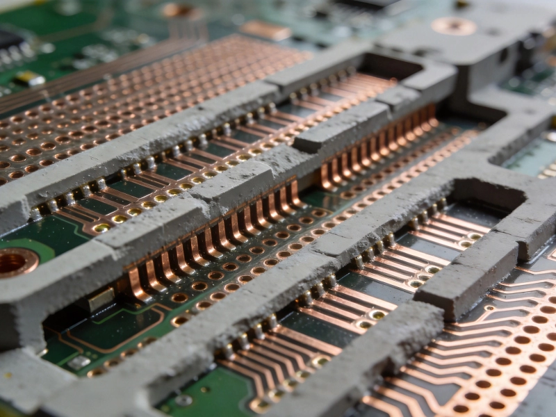
Designing Rugged HDI Boards for Harsh Industrial EnvironmentsJuly/20/2026
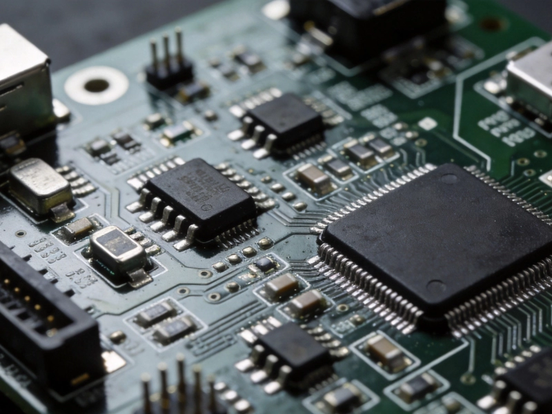
High-Reliability HDI Solutions for PLCs and Motor DrivesSeptember/16/2026
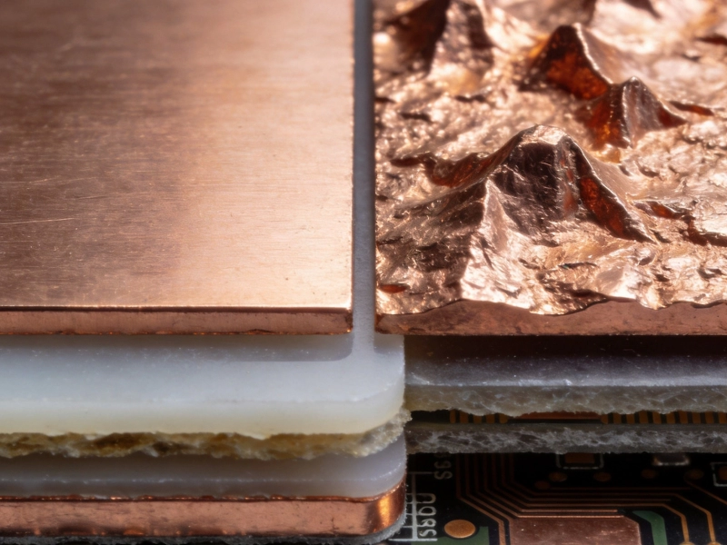
Understanding the Role of Copper Foil Roughness in Signal IntegritySeptember/23/2026
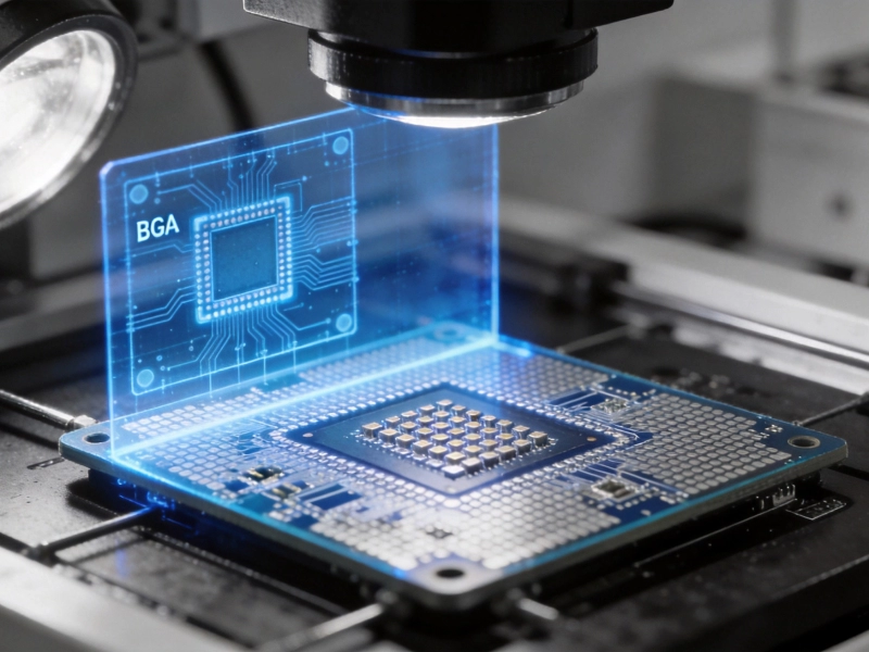
How X-Ray Inspection (AXI) Detects Hidden Defects in HDI BoardsJuly/30/2026
Exploring the 6 Types of HDI Structures: From Type I to Any-LayerAugust/14/2026
HDI Solutions for Wearable Health Monitors and Diagnostic ToolsSeptember/17/2026
HDI PCB Cost Guide: What Factors Drive the Price Up?June/16/2026
Conductive Anodic Filament (CAF) Resistance in High-Density BoardsJuly/31/2026