
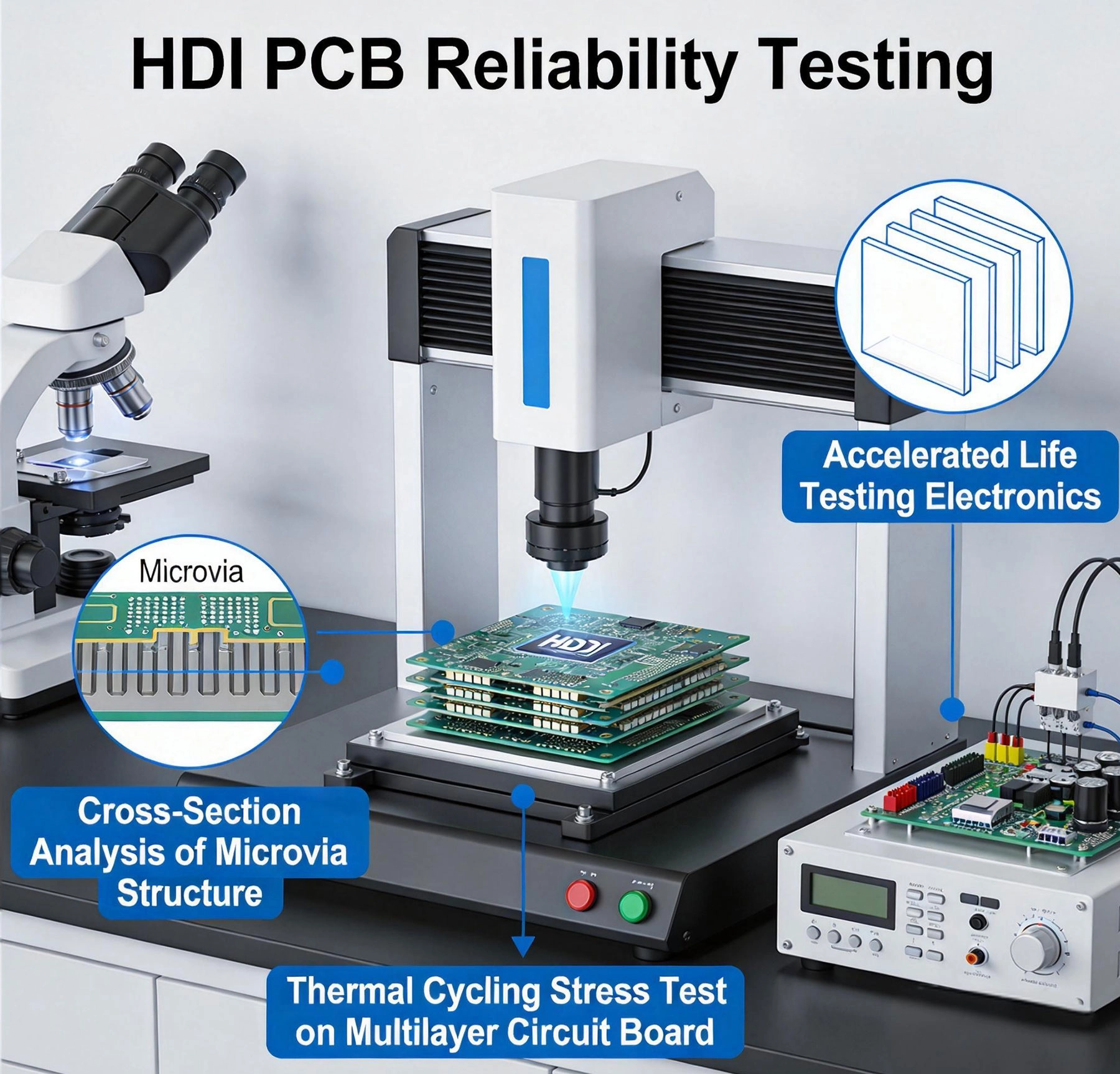
Every electronic product carries an implicit promise: it will work reliably for its intended service life. For a smartphone, that might mean 3-5 years of daily use. For an automotive electronic control unit, it's 15+ years and 150,000 miles of oper...
https://www.high-density-interconnect-pcb.comhttps://www.high-density-interconnect-pcb.com/energy-power-electronics/key-factors-influencing-the-long-term-reliability-of-hdi-pcbs/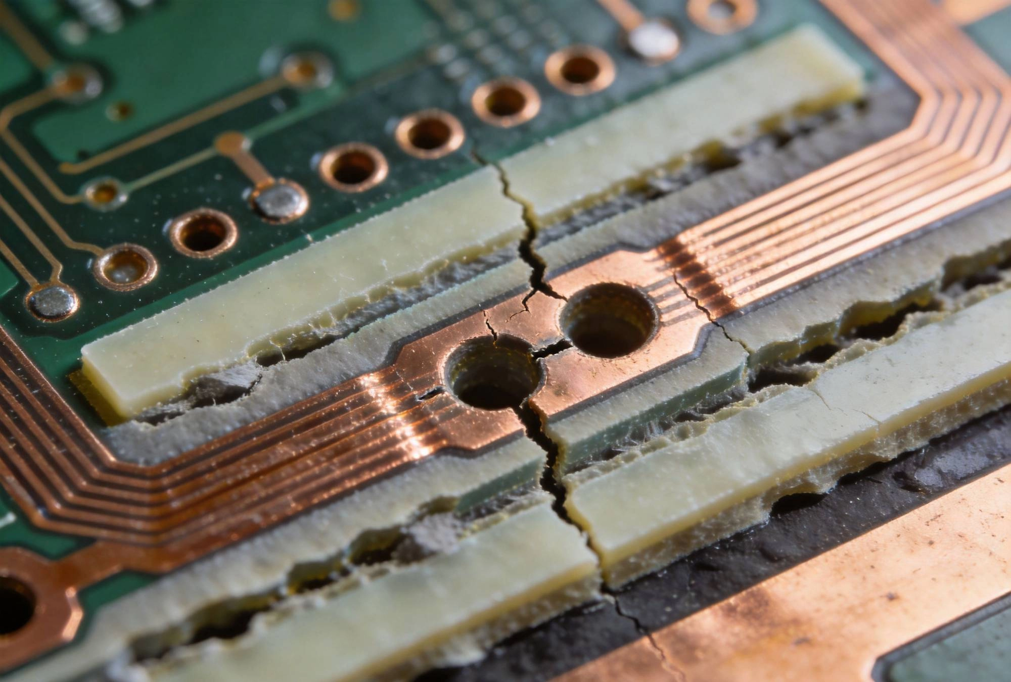
Modern electronic devices demand ever-increasing functionality packed into shrinking form factors. This relentless miniaturization drives the adoption of High-Density Interconnect (HDI) printed circuit board technologies, where microvias serve as t...
https://www.high-density-interconnect-pcb.comhttps://www.high-density-interconnect-pcb.com/hdi-pcb-reliability/understanding-and-preventing-microvia-cracking-in-thermal-cycling/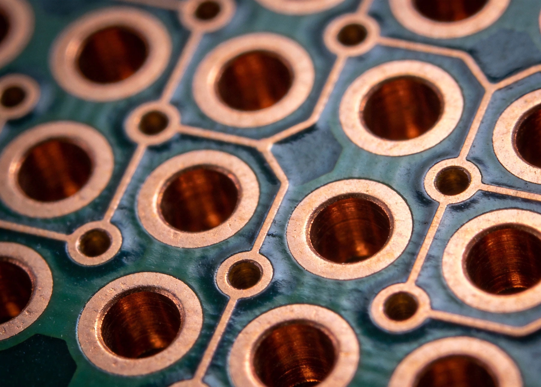
As PCB technology advances and device geometries shrink, the humble via—the plated hole that connects layers in a printed circuit board—has become one of the most critical and most vulnerable elements in modern electronics. Microvias, defined by th...
https://www.high-density-interconnect-pcb.comhttps://www.high-density-interconnect-pcb.com/hdi-pcb-design-testing/the-importance-of-electrical-testing-for-microvia-reliability/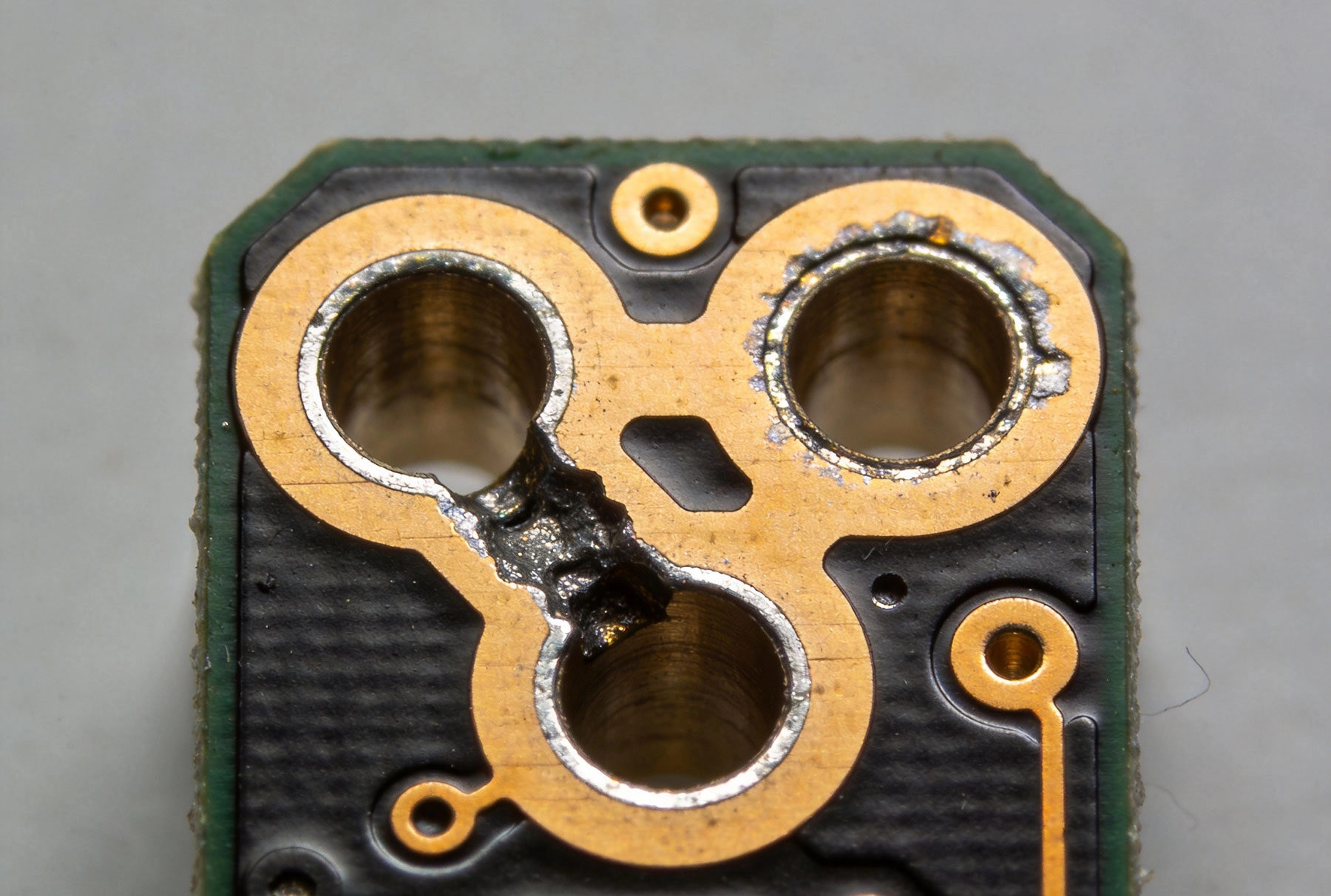
High-density interconnect (HDI) technology has revolutionized printed circuit board design by enabling unprecedented component density and signal performance. However, the sophisticated microvias and complex plating structures that make HDI possibl...
https://www.high-density-interconnect-pcb.comhttps://www.high-density-interconnect-pcb.com/hdi-pcb-reliability/the-impact-of-plating-voids-on-hdi-interconnect-reliability/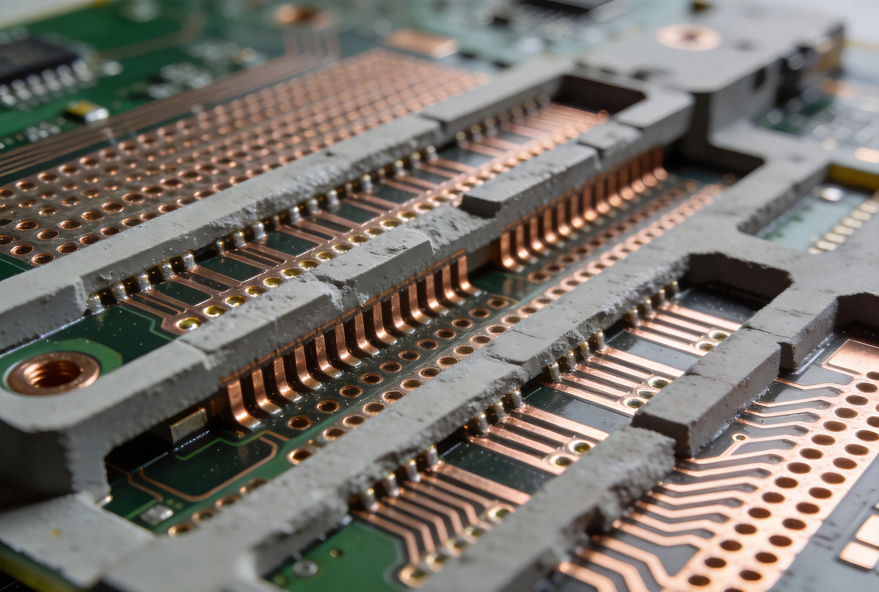
High Density Interconnect boards deliver remarkable functionality in compact packages—fine-pitch components, blind and buried vias, and dense routing that would be impossible in standard multilayer constructions. This capability comes with complexi...
https://www.high-density-interconnect-pcb.comhttps://www.high-density-interconnect-pcb.com/industrial-automation/designing-rugged-hdi-boards-for-harsh-industrial-environments/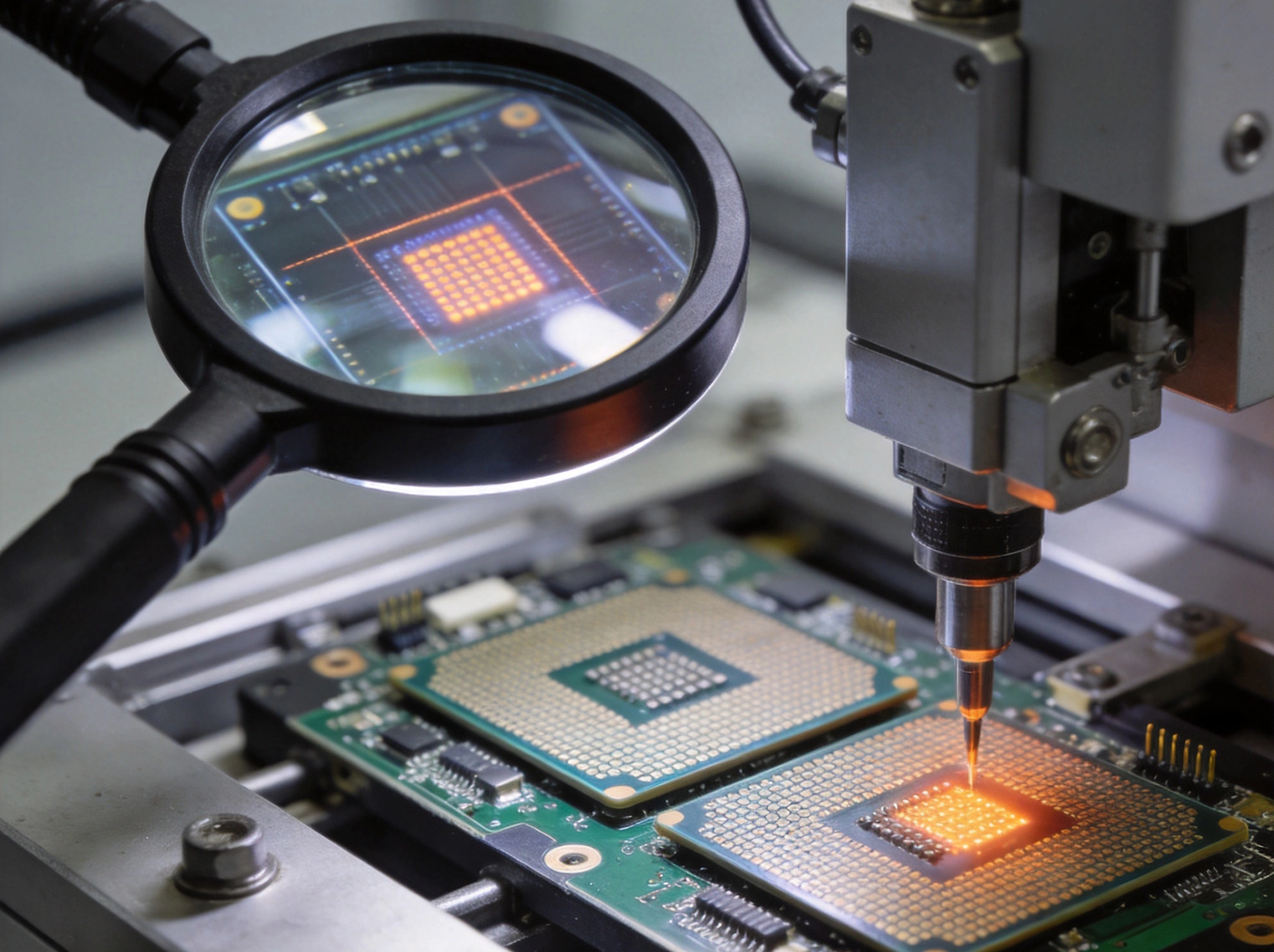
High Density Interconnect (HDI) printed circuit boards represent the pinnacle of miniaturization in electronics manufacturing. By utilizing microvias and fine-line geometries, HDI technology enables dramatically increased circuit density while redu...
https://www.high-density-interconnect-pcb.comhttps://www.high-density-interconnect-pcb.com/hdi-pcb-faq-support/troubleshooting-common-issues-in-hdi-pcb-assembly/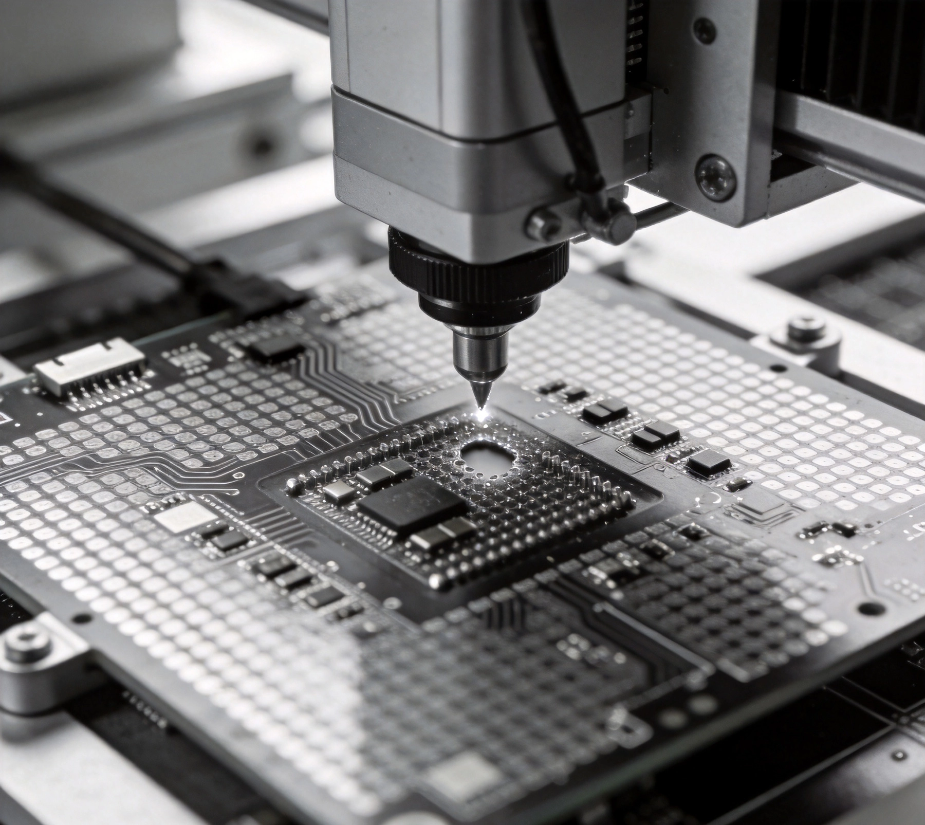
High-density interconnect (HDI) PCBs have transformed electronics manufacturing by enabling dramatically smaller, lighter, and more capable devices. From smartphones to medical implants, HDI technology makes possible what was impossible with trad...
https://www.high-density-interconnect-pcb.comhttps://www.high-density-interconnect-pcb.com/hdi-pcb-manufacturing/overcoming-common-manufacturing-defects-in-high-density-interconnects/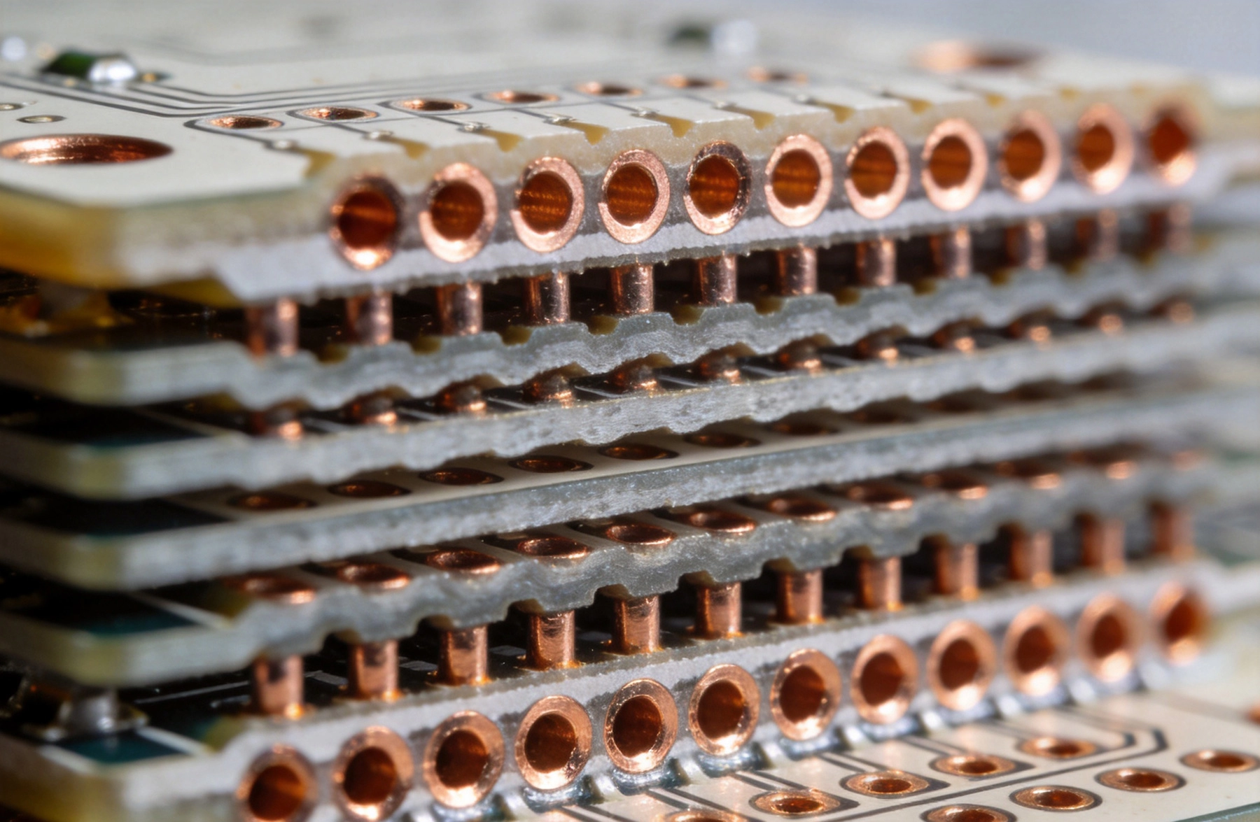
As electronics continue their relentless march toward miniaturization, high-density interconnect (HDI) technology has become standard practice rather than exotic exception. And at the heart of every HDI design lies the microvia—those laser-drilled,...
https://www.high-density-interconnect-pcb.comhttps://www.high-density-interconnect-pcb.com/hdi-pcb-design-testing/the-art-of-microvia-placement-staggered-vs-stacked-vias/