
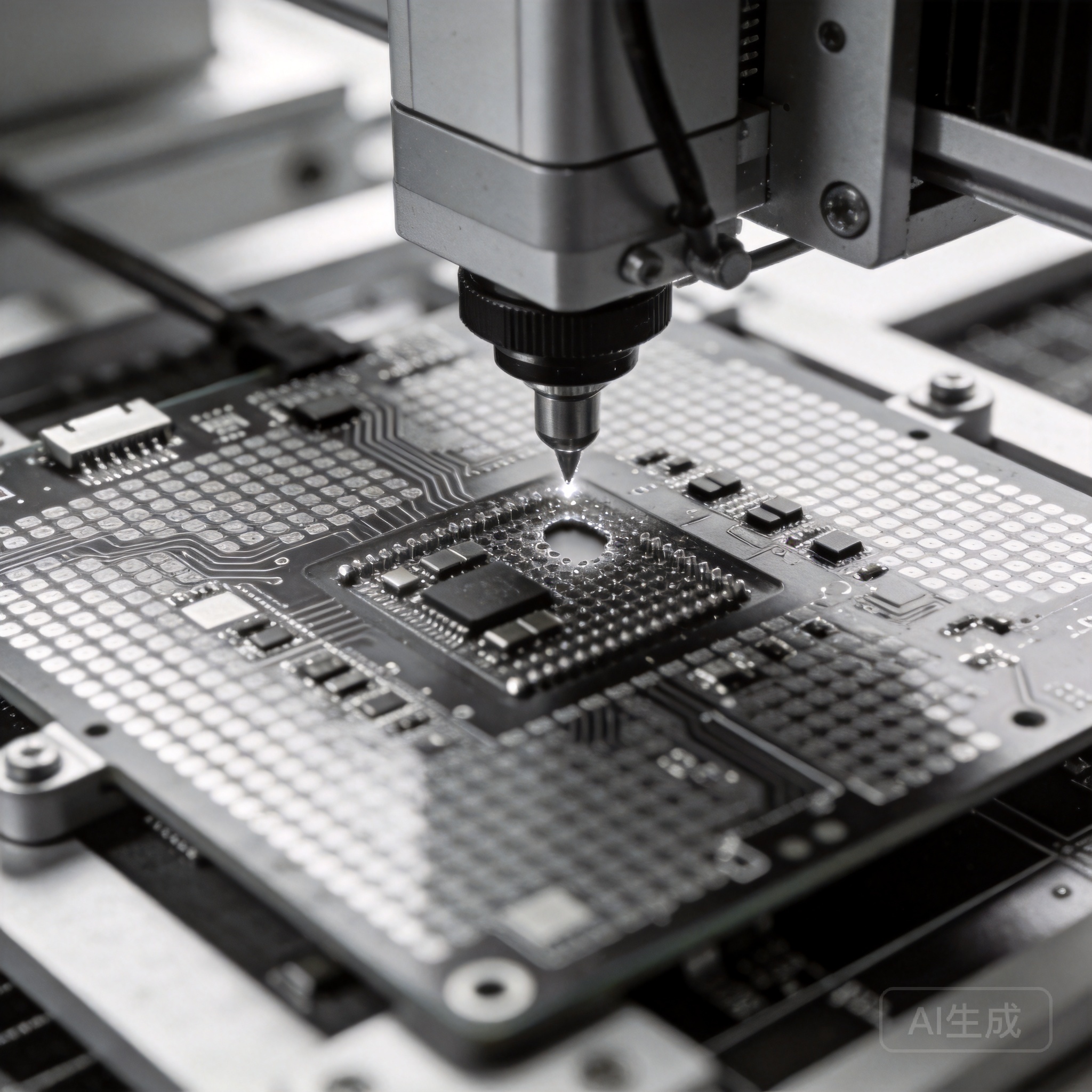
High-density Interconnect (HDI) PCBs have transformed Electronics Manufacturing by enabling dramatically smaller, lighter, and more capable devices. From smartphones to medical implants, Hdi Technology makes possible what was impossible with traditional board designs. Yet this Miniaturization comes at a cost: manufacturing complexity increases exponentially as feature sizes shrink. Defects that would be minor issues in conventional boards become catastrophic failures in HDI assemblies. Understanding these common defects and how to prevent them is essential for engineers and product managers working with advanced circuit board technology.
HDI PCBs push manufacturing boundaries across every dimension. Microvia diameters measured in fractions of a millimeter demand Laser Drilling precision. Trace widths approaching 50 microns require photolithography equipment operating at its limits. Layer-to-Layer Registration tolerances measured in microns challenge the mechanical precision of lamination and drilling processes. Each manufacturing step that works reliably for conventional boards becomes a potential failure point when feature sizes enter the HDI domain.
The consequences of HDI defects differ from conventional boards in both severity and detectability. A failed Microvia may affect functionality that depends on that specific connection, making diagnosis challenging. Defects may not manifest until thermal cycling, vibration, or aging reveals latent weaknesses. Understanding where defects originate and how they propagate helps teams implement effective prevention strategies.
Unlike standard Pcb Defects that often allow rework, many HDI defects are non-repairable due to the inaccessible nature of internal layers and microvia structures. When an internal microvia fails, the board must be scrapped. Scrap costs multiply rapidly because Hdi Boards typically contain expensive materials, require specialized processing, and have long fabrication cycles. A single defect discovered late in manufacturing can waste weeks of processing time and thousands of dollars in materials.
Defect escape to customers creates even larger costs through warranty claims, customer returns, and reputation damage. Hdi Boards typically serve applications where reliability is critical, making field failures particularly costly. Prevention through process control and early detection costs far less than the consequences of defective products reaching customers.
Microvias represent the defining feature of Hdi Technology, yet they also represent the most common source of reliability problems. These tiny laser-drilled vias connect adjacent layers with diameters typically ranging from 50 to 150 microns. Creating reliable connections through such small features challenges every aspect of the manufacturing process from drilling through plating to assembly.
Via barrel cracking occurs when thermal stress or mechanical loading fractures the Copper Plating inside the via. The high aspect ratio of deep Microvias makes achieving complete plating coverage difficult, leaving thin spots vulnerable to crack initiation. Thermal cycling during assembly and subsequent service creates cyclic stress that propagates cracks until the connection opens.
Via formation parameters directly affect reliability. Laser Drilling pulse energy, repetition rate, and spot size determine the quality of the drilled hole wall. Over-drilling or excessive pulse energy creates heat-affected zones with degraded plating adhesion. Optimized laser parameters that just penetrate the material minimize damage while creating clean holes ready for plating.
Plating chemistry and process control ensure complete copper deposition throughout the via barrel. High aspect ratio vias require specialized electroless copper processes that deposit evenly despite diffusion limitations. Pulse reverse plating balances coverage at via tops and bottoms, avoiding thin plating at either end. Bath analysis and maintenance keep chemistry within tight control limits that promote consistent plating quality.
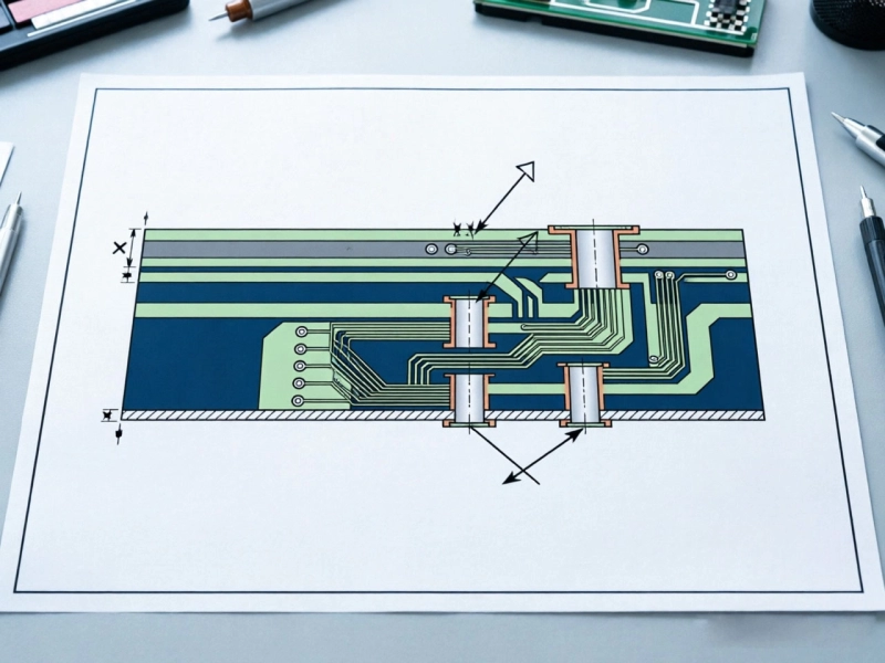
Board designers can influence Microvia Reliability through stackup and layout choices. Stacked Microvias, where vias from adjacent layers connect directly, create stress concentration points that are more vulnerable than staggered via arrangements. Staggered via designs distribute stress across a larger volume of material, improving overall reliability.
Via placement relative to high-stress areas reduces fatigue loading. Vias near board edges, mounting holes, or component pads experience higher stress concentrations. Routing traces away from these areas or adding support fillets distributes loading more evenly. Panel and array split orientation affects stress distribution during depanelization, influencing failure rates.
Ball grid array packages with pitches below 0.5mm present assembly challenges that escalate with Miniaturization. At 0.4mm pitch, individual solder balls measure approximately 0.25mm diameter with centers spaced just 0.4mm apart. Bridging between adjacent balls, insufficient solder volume for reliable joints, and misalignment beyond tolerance all threaten production yields and field reliability.
Head-in-pillow defects occur when partial wetting creates an apparently sound joint that actually has a gap between the component solder ball and the printed circuit pad. This defect may pass visual inspection and even basic electrical testing while remaining vulnerable to intermittent failure under thermal or mechanical stress. The gap creates high resistance that generates heat during operation, potentially progressing to catastrophic failure.
Stencil aperture design determines solder volume and print quality for BGA assembly. Aperture size relative to pad dimensions affects solder deposit volume. Aperture shape influences paste release from stencil walls. For 0.4mm pitch BGAs, laser-cut stencils with polished walls provide the best paste release characteristics.
Stencil thickness balances solder volume against bridging risk. Thicker stencils provide more solder for robust joints but increase bridging tendency between closely spaced balls. Advanced stencil technologies including electroformed nickel and nanocoatings improve release efficiency, allowing adequate solder volume without increasing thickness. Step stencils with different thicknesses under BGAs versus peripheral components optimize process windows for mixed feature sizes.
Reflow profile directly affects joint formation quality. Preheating ramp rates that are too slow allow flux to exhaust before solder melting, reducing wetting force. Excessive peak temperatures damage components or create excessive intermetallic layers. Cooling rates that are too slow coarsen grain structure and weaken joints.
For fine-pitch BGAs, nitrogen atmosphere reflow often provides meaningful yield improvements. Oxygen in the reflow atmosphere oxidizes solder and pad surfaces, reducing wetting forces and promoting head-in-pillow defects. Nitrogen atmosphere suppresses oxidation, improving wetting and reducing defect rates when combined with clean surfaces and optimized profiles.
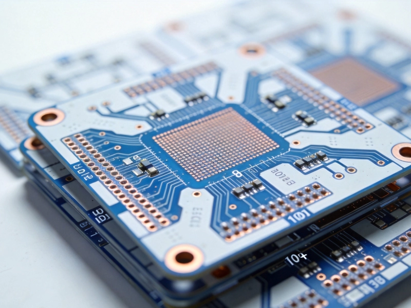
HDI boards with multiple Sequential Lamination cycles accumulate registration error with each layer addition. A board with six build-up layers might accumulate registration errors of 50 microns or more if each lamination step introduces just 10-15 microns of drift. This cumulative error can exceed tolerance budgets for fine-pitch components, causing misregistration that prevents reliable assembly.
Layer shift during lamination occurs when prepregs soften and flow, allowing copper features to move relative to each other. Large copper features create drag forces that pull against resin flow during lamination. Asymmetric panel layouts or unbalanced copper distribution intensify these forces, creating non-uniform shift patterns that are difficult to predict.
Panel preparation significantly affects lamination registration. Clean panel surfaces without contamination ensure consistent resin adhesion. Panel flatness and thickness uniformity reduce variability in press performance. Stress relief procedures before drilling and routing prevent built-in distortion from propagating through subsequent processes.
Lamination press parameters influence registration stability. Slow closing speeds reduce impact forces that shift layers during initial contact. Distributed filling of press blanks ensures uniform pressure application. Press temperature and pressure profiles that minimize early flow when resin viscosity is lowest reduce layer movement during critical bonding stages.
Designer choices affect board susceptibility to registration issues. Distributing copper evenly across the panel reduces unbalanced forces that pull layers during lamination. Breakaway tabs and timing holes provide mechanical references that help maintain alignment through processing. Anti-pad sizing accounts for expected registration tolerance, preventing Annular Ring reduction that would create registration-sensitive features.
Panel utilization strategies affect registration stability. Manufacturing panels with multiple product arrays can introduce variability as individual arrays respond differently to processing stress. Dedicated panels for HDI products allow process optimization without compromise for standard board requirements. Standardizing on common panel sizes reduces changeover time and maintains consistent process conditions.
Delamination between PCB layers represents a catastrophic failure mode where previously bonded surfaces separate under thermal or mechanical stress. This defect exposes internal circuits, creates open connections, and may progress to complete board failure. Delamination in HDI boards often originates at features like Buried Vias or large reference planes where interfacial strength is reduced.
Laminate voids are gas pockets trapped between layers during lamination. These voids create stress concentration points that weaken the board structure and may expand under thermal loading until they reach critical size. Voids near signal layers may affect Impedance Control, while voids near thermal paths reduce heatsinking effectiveness.
Surface contamination is a primary cause of delamination. Oxides, fingerprints, oils, and manufacturing residues all reduce interfacial bonding strength. Strict handling procedures, chemical cleaning processes, and careful storage of prepreg materials prevent contamination introduction. Automated handling systems reduce human contact with critical surfaces during panel processing.
Oxide treatment of copper surfaces balances adhesion against material degradation. Light oxide provides excellent bonding through mechanical interlocking and chemical bonding. Excessive oxide becomes brittle and can crack under thermal stress, creating delamination initiation sites. Automated oxide control systems maintain consistent oxide weights within tight specifications.
Vacuum lamination eliminates air entrapment that creates voids. Full vacuum before pressure application allows air to escape from intricate HDI structures before material flows close the panel gap. Progressive pressure application forces material into cavities without trapping gas pockets. Vacuum-assisted processes are essentially mandatory for HDI boards with fine features.
Temperature ramp rates during lamination affect resin flow and bonding. Too-fast heating causes premature gelation before pressure fully compresses the layup. Too-slow heating allows excessive resin flow that can wash small features out of position. Optimized profiles maintain material in the proper viscosity range for complete consolidation before gelation occurs.
Electroplated copper provides the current-carrying conductor through vias and on surface layers. Achieving uniform plating through the high aspect ratio features common in HDI boards challenges conventional plating processes. Voids in via barrels create current constrictions that generate heat and accelerate electromigration failure. Thin copper on surface features reduces current-carrying capacity and mechanical strength.
Conformal plating attempts to deposit copper uniformly on all exposed surfaces regardless of feature geometry. This approach often leaves thin spots in via barrels and at corners where current density concentrates. Sequential plating that deposits copper in stages with intermediate buffing steps can improve coverage, but adds process complexity and cost.
Pulse reverse plating modulates current direction and magnitude to improve plating distribution. Forward pulses deposit copper while reverse pulses dissolve material from high-current-density areas, balancing coverage across complex geometries. Careful optimization of pulse parameters, duty cycle, and current density achieves coverage difficult or impossible with direct current plating.
Selenium and alternative chemistries offer superior throwing power compared to conventional acid copper processes. These proprietary formulations extend the range of feature sizes that can be plated uniformly in a single process. Investment in advanced plating chemistry provides returns through improved yields and reduced scrap from plating-related failures.
Microvia cross-section analysis verifies plating quality during process qualification and periodically during production. Samples prepared from production panels show actual plating thickness distribution through via barrels. Automated image analysis quantifies uniformity and identifies trends before out-of-specification conditions develop.
Electrical test for continuity and isolation detects plating opens and shorts that result from extreme plating defects. High voltage testing at potentials above operating conditions may detect latent weaknesses like thin plating that will fail prematurely in service. Continuity test after each lamination stage identifies defects early when rework is still possible.
Fine-line etching becomes increasingly challenging as trace widths shrink toward 50 microns and below. Over-etching narrows traces beyond tolerance, reducing current-carrying capacity and creating impedance variations. Under-etching leaves tie bars and shorts between traces, requiring rework that may damage adjacent features. The tolerance budget for etching errors shrinks as feature size decreases, demanding tighter process control.
Etch factor, the ratio of etch depth to lateral undercut, determines minimum trace spacing achievable with a given process. Low etch factor processes create trapezoidal traces with significant width reduction. Higher etch factor processes approach vertical sidewalls, maintaining trace width closer to photolithography dimensions. HDI features require high etch factor processes to maintain acceptable geometry.
Photoresist application uniformity affects critical dimension control across the panel. Spray application provides better conformality over topographical features compared to curtain coating. Film resists offer the highest resolution for features below 50 microns, with consistent thickness control that translates to predictable etch results.
Exposure energy and development parameters determine feature geometry and edge quality. Underexposure leaves resist with reduced durability for subsequent processing. Overexposure creates rounded profiles and reduces resolution. Automated developer monitoring maintains consistent development rates across panels and across lots.
Plasma etching, also called reactive ion etching, provides near-vertical sidewalls with minimal undercut. This anisotropic process removes material preferentially in the vertical direction, approaching photolithography-defined dimensions in the final trace. However, plasma etching equipment and process development require significant investment compared to conventional spray etching.
Pattern plating deposits copper only where needed rather than etching away unwanted material. This additive approach eliminates etch factor concerns entirely, achieving trace widths limited only by photolithography resolution. Pattern plating processes require additional steps including seed layer deposition and etch resist stripping, but the dimensional advantages make it attractive for the finest HDI features.
Surface finish quality directly affects assembly yield and solder joint reliability. Uneven finish thickness creates inconsistent wetting behavior during assembly. Porous finishes allow oxidation to reach underlying copper, degrading solderability during storage. Incomplete coverage exposes copper that may corrode or create voids during solder reflow.
For HDI boards with fine features, the ENIG process is popular for its excellent flatness and shelf life. However, nickel diffusion and gold porosity can create assembly problems. Electroless nickel immersion gold requires careful process control to achieve the proper nickel thickness and phosphorus content that ensures reliable performance. Alternative finishes including immersion silver and OSP each have specific process windows that must be maintained.
Finish selection should consider storage conditions, assembly processes, and performance requirements. Boards stored for extended periods before assembly may benefit from ENIG's superior shelf stability. Boards assembled immediately after receipt may use less expensive finishes that still provide excellent assembly results. Performance requirements like wire bonding or multiple reflow cycles influence finish choice.
Process specification should address the parameters critical to each finish type. ENIG nickel thickness affects diffusion barrier effectiveness and solder joint integrity. Immersion silver thickness affects oxidation rate and shelf life. OSP coating weight affects protection duration and reflow tolerance. Specifying ranges rather than single targets allows manufacturers to optimize within acceptable windows.
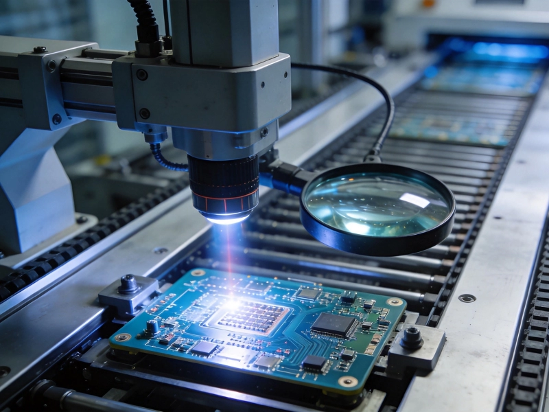
Preventing HDI defects requires systematic approach spanning design, manufacturing, and Quality Control. Defect prevention starts with design practices that accommodate manufacturing variability, continues through process control that maintains stable manufacturing conditions, and concludes with inspection systems that detect defects before they propagate to subsequent processes or reach customers.
Statistical process control provides early warning of process drift before defects occur. Tracking key process parameters including plating thickness, registration, and etch critical dimensions reveals trends that might indicate approaching out-of-specification conditions. Proactive adjustment based on statistical control limits prevents defects rather than merely detecting them.
Supplier qualification for HDI boards requires more extensive evaluation than standard PCB qualification. Process capability studies verify that manufacturers can achieve the tolerances HDI products require. First article inspection provides detailed comparison of prototype boards against specifications. Process qualification audits verify that quality systems and process controls are in place and functioning.
Ongoing monitoring through regular sampling and testing maintains confidence in supplier performance. Certificate of conformance alone is insufficient for high-reliability applications. Participation in supplier quality programs, including shared defect data and corrective action collaboration, builds partnerships that improve quality over time.
Manufacturing High-density Interconnect PCBs presents genuine challenges that demand investment in equipment, process development, and quality systems. The seven defect categories examined here represent the most common failure modes encountered in HDI production, each requiring specific prevention strategies and detection methods.
Successful Hdi Manufacturing requires collaboration between designers who understand manufacturing capabilities and limitations and manufacturers who have invested in the equipment and expertise necessary for fine-feature processing. Early engagement between design and manufacturing teams identifies potential problems while design changes are still inexpensive to implement.
The payoff for mastering Hdi Manufacturing challenges is access to markets and applications that require miniaturization, high performance, and reliability. From medical devices that improve patient outcomes to mobile devices that connect billions of people, HDI technology enables electronic products that transform how we live and work. Understanding and overcoming the manufacturing defects that challenge HDI production is essential for engineers and companies seeking to compete in these demanding applications.
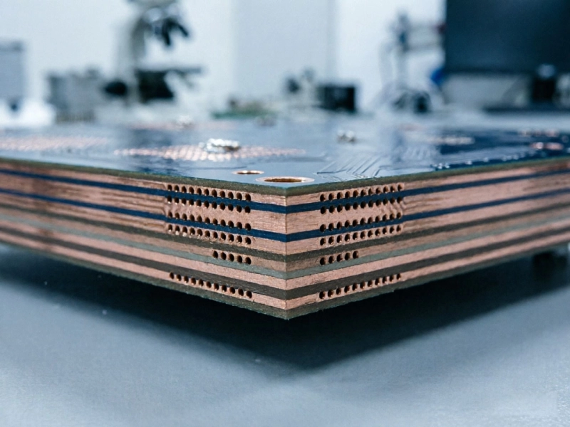
Understanding Sequential Lamination in Multi-Step HDI BoardsJuly/03/2026
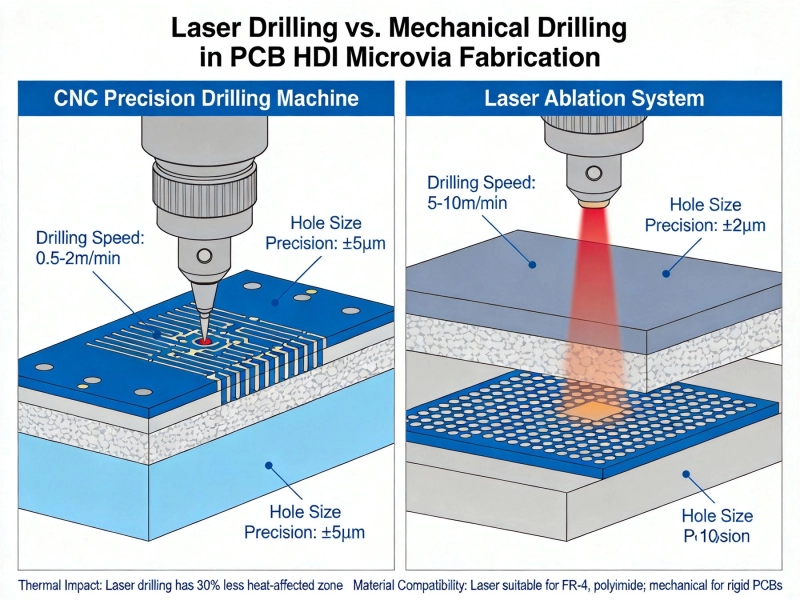
Precision in HDI FabricationJune/04/2026

What is the Lead Time for Manufacturing Custom HDI Boards?October/12/2026
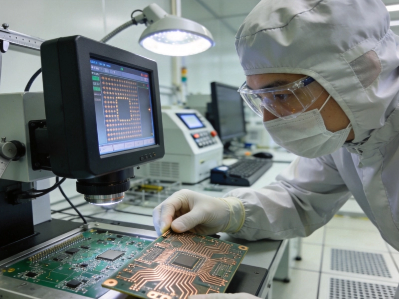
The Challenge of Plating and Filling Microvias in HDI ProductionJuly/26/2026
Critical Quality Checkpoints in the HDI Production LineJuly/13/2026
How Manufacturers Achieve High Precision Alignment in 10+ Layer HDI BoardsAugust/15/2026
How HDI Technology Supports PCIe Gen5 and Gen6 ComputingSeptember/15/2026
How to Read and Interpret HDI PCB Stack-up Drawings?July/14/2026