
High Density Interconnect (HDI) printed circuit boards represent the pinnacle of Miniaturization in Electronics Manufacturing. By utilizing Microvias and fine-line geometries, Hdi Technology enables dramatically increased circuit density while reducing board size and weight. However, these same characteristics that make HDI so powerful also create unique assembly challenges that differ significantly from conventional PCB assembly. Issues that would be minor problems on standard boards can become catastrophic failures in HDI assemblies.
This guide provides systematic approaches to identifying and resolving common Hdi Pcb assembly problems. Understanding these challenges and their solutions helps engineers design more manufacturable products and enables production teams to respond effectively when issues arise.
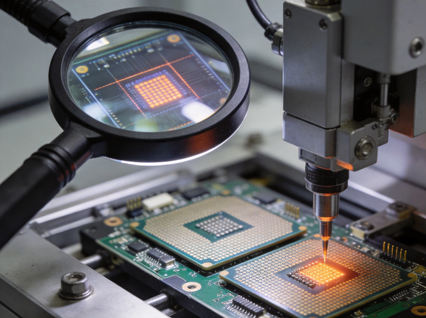
Hdi Boards present assembly challenges that stem from their fundamental construction. Before troubleshooting specific issues, understanding these complexities provides context for effective problem resolution.
Hdi Technology employs features that create manufacturing considerations:
Each feature introduces potential failure modes not present in conventional board assembly.
The high component density typical of HDI assemblies creates interaction effects:
Microvias form the foundation of HDI technology but present unique reliability challenges that require specific troubleshooting approaches.
Common Microvia failure mechanisms include:
When Microvia failures occur, systematic investigation identifies root causes:
Address Microvia Reliability through design and process improvements:
Hdi Boards typically utilize BGA and other fine-pitch packages that present assembly challenges. These components demand precision beyond standard SMT requirements.
BGA packages require placement accuracy exceeding standard SMT tolerance:
Placement systems must be properly calibrated and maintained for HDI assembly.
Voids in solder joints under BGA packages create reliability concerns:
Void control requires attention to solder paste formulation, printing parameters, and reflow profile optimization.
Hidden joints beneath BGA packages are invisible to optical inspection:
HDI assembly demands solder paste printing precision exceeding standard requirements. Printing issues cascade through subsequent assembly steps.
Stencil selection and design critically affects HDI printing:
Advanced stencils with tapered walls and electropolished surfaces improve paste transfer efficiency.
Typical printing problems affecting HDI assemblies:
Optimize printing through parameter adjustment:
Reflow thermal profiles require optimization for HDI assemblies due to their thermal mass characteristics and component density.
HDI thermal profiles must balance multiple requirements:
The thermal mass of HDI boards differs from conventional boards, requiring profile adjustment.
Thermal profile issues manifest as specific defects:
Systematic profile development improves outcomes:
HDI boards utilize specialized materials that require attention to handling and processing requirements.
HDI materials often have stringent moisture sensitivity requirements:
Track shelf life and storage conditions to prevent moisture-related failures.
Material combinations in HDI boards must be compatible:
Testing HDI assemblies presents unique challenges due to high density and small features.
h3>Probe AccessibilityTest access becomes difficult with HDI density:
Balance test coverage against board real estate:
Systematic yield improvement reduces cost and improves quality in HDI assembly.
Effective troubleshooting requires good data:
Systematic investigation approaches:
Many HDI assembly issues can be prevented through better design practices.
Follow HDI-specific DFM guidelines:
Early manufacturer involvement prevents issues:
Troubleshooting Hdi Pcb assembly requires understanding the unique challenges of high-density technology:
Successful HDI assembly requires close collaboration between design engineers and manufacturing specialists. Early identification of potential issues enables proactive resolution before they impact production yield.
The most common HDI assembly defects include BGA misalignment and bridging, microvia failures from inadequate plating or thermal stress, void formation under BGA packages, solder paste printing defects from stencil issues, and delamination from moisture absorption or thermal excursion.
Prevent microvia failures by specifying adequate plating thickness, using reputable manufacturers with proven process capability, designing appropriate microvia structures for your application, and avoiding thermal profiles that stress via structures beyond their capability.
HDI assemblies require X-ray Inspection for hidden joints under BGAs, 3D Automated Optical Inspection for visible features, solder paste inspection before reflow, and cross-sectioning for internal quality verification. Standard visual inspection is insufficient due to component density.
Optimize HDI thermal profiles by collecting thermal data from multiple board locations, adjusting ramp rates to minimize thermal gradients, balancing peak temperature against component and material limits, and using soak periods appropriate for board thermal mass.
HDI assembly requires laser-cut stencils with smooth aperture walls, nano-coating for improved paste release, appropriate thickness matched to pad size requirements, and tension specifications suitable for fine-feature printing.
HDI materials often have stricter moisture sensitivity levels due to laser-abraded surfaces that create moisture ingress pathways. More aggressive dry storage and baking requirements may apply. Always verify MSL ratings with your manufacturer.
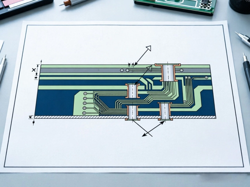
How to Read and Interpret HDI PCB Stack-up Drawings?July/14/2026
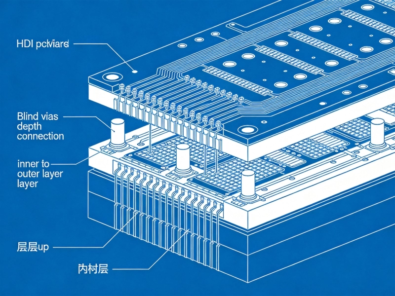
Understanding HDI Terminology: A Glossary for EngineersAugust/03/2026
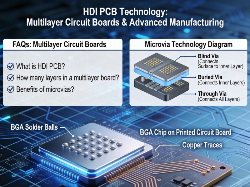
Top 10 Frequently Asked Questions About HDI PCB TechnologyMay/28/2026
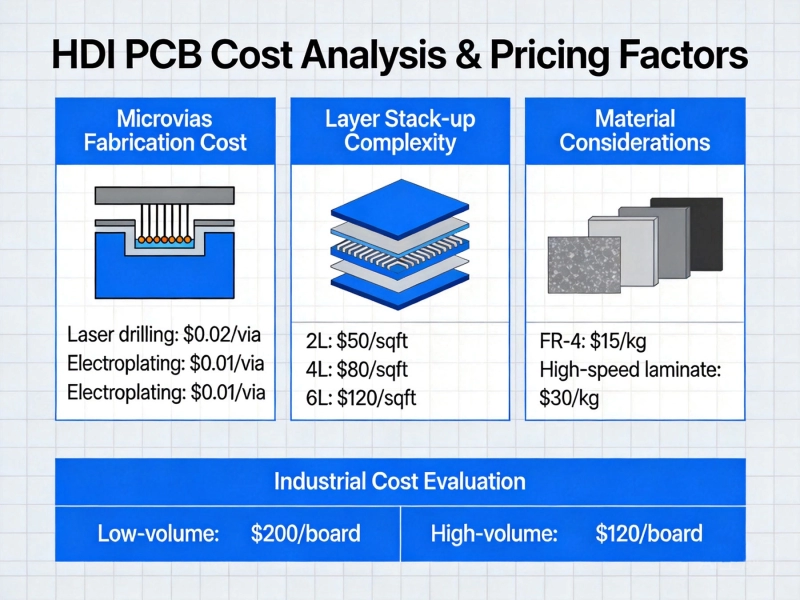
HDI PCB Cost Guide: What Factors Drive the Price Up?June/16/2026
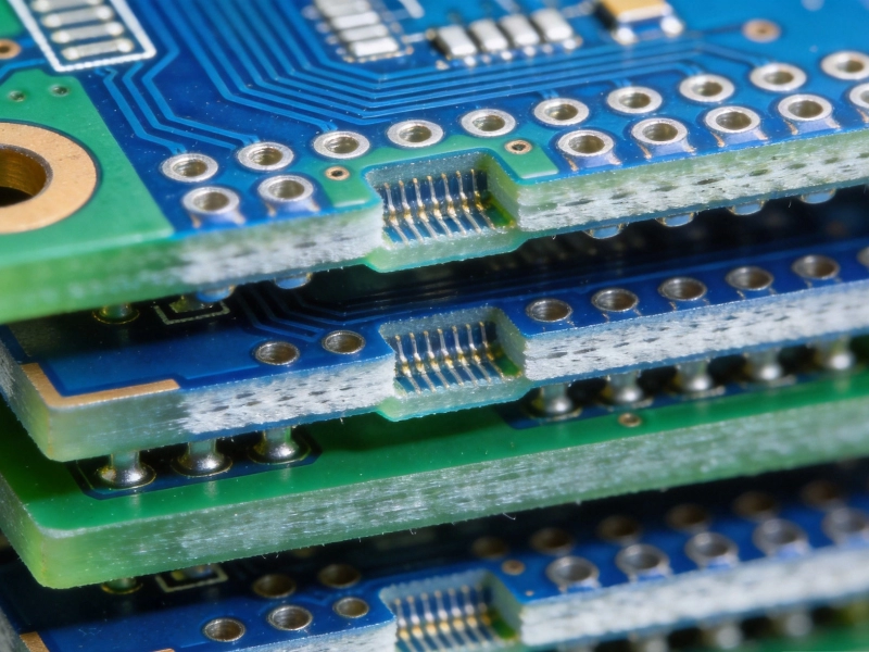
An Introduction to Microvia Technology in HDI PCBsJuly/24/2026

Implementing a Robust Quality Control System for HDI ManufacturingJune/15/2026
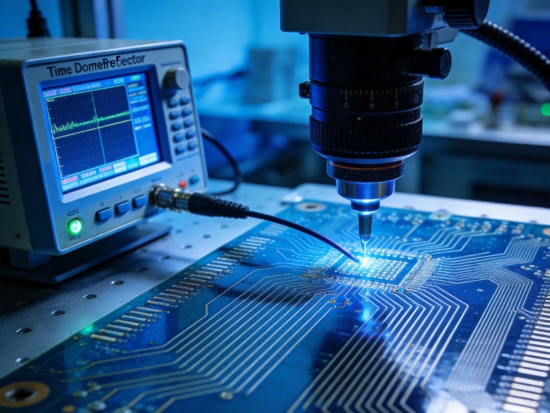
How to Measure and Control Impedance Tolerance in HDI BoardsAugust/03/2026
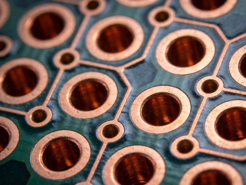
The Importance of Electrical Testing for Microvia ReliabilityJuly/09/2026