Open Nav

High Density Interconnect (HDI) technology has revolutionized Pcb Design by enabling higher component density, smaller form factors, and improved electrical performance. However, the specialized manufacturing processes and design techniques associated with HDI have introduced terminology that can confuse even experienced engineers. Clear understanding of HDI terminology becomes essential for effective communication between design teams and manufacturing partners. This glossary provides comprehensive definitions of the most important HDI terms, enabling engineers to specify requirements accurately and interpret manufacturing feedback correctly.
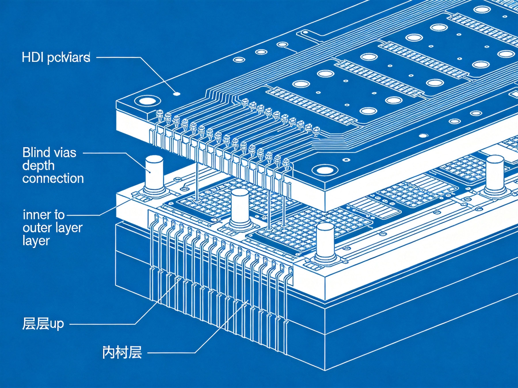
Microvias represent the defining feature of Hdi Technology. These are laser-drilled vias with diameters typically 150 micrometers or smaller, enabling dense component placement and improved electrical performance. Microvias allow routing between adjacent layers without consuming the area required for mechanically drilled through-holes. The small size and tight pitch of microvias enable routing densities 5 to 10 times higher than possible with conventional vias.
Two primary Microvia Drilling technologies exist: laser drilling for dielectric materials and mechanical drilling for very small diameters. Laser drilling provides superior precision and enables blind and Buried Via formation that would be impossible with mechanical drilling. The aspect ratio of microvias—depth to diameter ratio—typically ranges from 0.75:1 to 1:1, which is significantly shallower than through-hole vias and contributes to improved reliability.
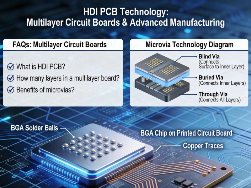
Blind Vias connect an outer layer to one or more inner layers without passing completely through the board. This structure enables component placement on both sides of the board while maintaining interior routing capability. Blind Vias reduce layer count requirements by providing direct connections to inner layers, which is particularly valuable in dense designs where routing space is at a premium.
Blind vias can be either through-hole vias drilled from one side that do not penetrate the entire board thickness, or laser-drilled microvias that terminate at a specific inner layer. The depth control required for blind vias demands precise drilling and plating processes. When specifying blind vias, designers must identify the start layer and target layer, typically using notation like "L1-L3" to indicate a via starting on layer 1 and terminating on layer 3.
Buried Vias connect inner layers without reaching either outer surface of the board. These vias are completely encapsulated within the board structure, providing interlayer connections without consuming surface area for component placement. Buried Vias enable complex multilayer routing strategies that would be impossible if all vias required access to outer surfaces.
The fabrication of buried vias requires Sequential Lamination processes where inner layer sub-assemblies are created, drilled, plated, and then combined with additional layers. This sequential build-up process represents a key differentiator between HDI fabrication and standard multilayer board manufacturing. Buried vias typically follow a layer-to-layer connection pattern, connecting adjacent layers or spanning multiple inner layers as required by the routing scheme.
Through-hole vias penetrate the entire board thickness, connecting all layers from top to bottom. While not exclusive to Hdi Technology, through-hole vias remain important even in HDI designs for applications requiring mechanical strength, Thermal Conductivity, or compatibility with through-hole components. Hdi Boards often mix through-hole vias with microvias, using each type where its characteristics provide the best advantage.
Through-hole vias in Hdi Boards often incorporate back-drilling to remove unused barrel portions that would create stub effects. These back-drilled vias, sometimes called controlled depth vias or stubless vias, improve Signal Integrity for high-speed applications by eliminating the impedance discontinuity created by unused via barrels.
Sequential Lamination describes the process of building HDI boards through multiple lamination cycles rather than the single lamination cycle used for standard multilayer boards. Each lamination cycle adds new layers and creates new via structures. This process enables the creation of blind and buried vias that would be impossible to fabricate in a single lamination step.
A typical sequential lamination process might start with a double-sided core, add two build-up layers on each side with laser-drilled microvias, laminate and plate, then add additional build-up layers in subsequent cycles. The number of lamination cycles determines the maximum layer count and via depth that can be achieved. More cycles enable higher layer counts but increase process complexity and cost.
Build-up layers refer to the dielectric and copper layers added during sequential lamination cycles. These layers typically use thin dielectric materials that enable fine-pitch laser drilling and controlled impedance. Common build-up materials include ABF (Ajinomoto Build-up Film), epoxy-based dielectrics, and other materials formulated specifically for Hdi Applications.
The thickness of build-up layers typically ranges from 2 to 4 mils for Dielectric Material plus 0.5 to 1 mil for copper foil. These thin dimensions enable high routing density and tight Impedance Control. However, thin layers also increase sensitivity to dimensional variations, requiring tighter process control compared to standard multilayer boards.
The core material provides the structural foundation for HDI boards, typically consisting of a dielectric layer with copper cladding on both sides. Core materials generally use standard FR4 or similar substrates with thickness ranging from 4 to 20 mils depending on the application requirements. The core provides mechanical stability and forms the starting point for sequential build-up processes.
Core selection impacts electrical and thermal performance. Thicker cores provide better Thermal Conductivity and mechanical rigidity but increase overall board thickness. High-frequency applications may use low-loss core materials like Rogers laminates, while cost-sensitive applications typically use standard FR4 cores.
The layer stackup defines the arrangement of dielectric and copper layers in the completed board, including the sequence of materials, layer thicknesses, and copper weights. HDI stackups typically follow symmetrical patterns to prevent warping, though asymmetrical designs exist for specific applications. The stackup determines impedance characteristics, routing density, and overall board thickness.
Stackup notation typically identifies each layer by number and material type. For example, "L1 (top copper), D1 (dielectric), L2 (inner copper), Core, L3 (inner copper), D2 (dielectric), L4 (bottom copper)" describes a 4-layer board. HDI stackups include additional build-up layers, with notation like "Build-up Layer 1, L1, Dielectric 1, L2, Core, L3, Dielectric 2, L4, Build-up Layer 2, L5."
Via-in-pad describes the technique of placing vias directly within component pads rather than offsetting them to the side. This approach eliminates the annular ring area around the via, allowing tighter component spacing and reducing the area required for ball grid array (BGA) and other fine-pitch components. Via-in-pad also reduces inductance compared to conventional via placement, improving electrical performance at high frequencies.
Implementing via-in-pad requires additional processing steps. After drilling and plating, the via must be filled with conductive or non-conductive material and planarized to create a flat surface for component soldering. The filling process can use electroplated copper, conductive epoxy, or non-conductive epoxy depending on the electrical and thermal requirements.
Copper-filled vias provide both electrical connectivity and thermal conductivity. The electroplating process completely fills the via barrel with copper, creating a solid conductive path from one layer to another. Copper filling provides excellent thermal conductivity for Heat Dissipation and creates a flat surface that is compatible with surface mount component soldering.
The copper filling process adds cost and process complexity compared to standard plating. Filled vias require additional plating time and careful process control to ensure complete fill without voids. However, the benefits for Thermal Management and electrical performance justify the additional cost in many applications.
Epoxy filling provides mechanical support and surface planarization without the electrical conductivity of copper filling. Epoxy-filled vias can be either conductive or non-conductive depending on the epoxy formulation. Conductive epoxy fills maintain electrical connectivity, while non-conductive fills isolate the via barrel electrically while providing mechanical support.
Epoxy filling typically costs less than copper filling and provides adequate performance for many applications. The filling process is simpler and requires less plating time. However, epoxy-filled vias do not provide the thermal conductivity benefits of copper-filled vias, making them less suitable for power applications.
Signal Integrity refers to the quality of electrical signals as they propagate through transmission lines. In HDI designs, signal integrity becomes increasingly critical because shorter trace lengths and higher component density create more opportunities for interference and reflection. Maintaining signal integrity requires careful Impedance Control, proper termination, and minimization of discontinuities.
HDI technology often improves signal integrity compared to standard designs because shorter traces reduce signal attenuation and microvias create less inductance than through-hole vias. However, the tight spacing of traces and vias increases the potential for crosstalk, requiring careful design and layout practices.
Crosstalk occurs when signals on adjacent traces couple electromagnetically, causing unwanted signal transfer. The close spacing of traces in HDI designs increases crosstalk potential. Two types of crosstalk exist: capacitive coupling, which occurs through electric fields, and inductive coupling, which occurs through magnetic fields. Both types can create signal integrity problems in high-density designs.
Mitigating crosstalk in HDI designs requires techniques including ground reference planes between signal layers, increased trace spacing where possible, differential signaling for critical signals, and careful layer stackup design that minimizes coupling between adjacent signal layers.
Controlling EMI in HDI designs involves proper ground plane design, controlled impedance transmission lines, decoupling capacitors placed close to power pins, and shielding where necessary. The compact nature of HDI boards can actually help with EMI containment when proper layout practices are followed, because shorter traces act as less efficient antennas.
Aspect ratio describes the relationship between the depth of a via and its diameter. Higher aspect ratios create more challenging plating and drilling processes. Standard through-hole vias might have aspect ratios of 8:1 or higher, while microvias typically range from 0.75:1 to 1:1. The shallower aspect ratio of microvias contributes to better plating reliability and enables the use of fine-pitch features.
Aspect ratio becomes particularly important for reliability considerations. Higher aspect ratios make complete plating more difficult and increase the risk of Plating Voids. When specifying via sizes, designers should consider the aspect ratio implications for manufacturability and reliability.
Yield refers to the percentage of finished boards that meet quality specifications without requiring rework or scrap. HDI boards typically have lower yields than standard boards due to increased process complexity and tighter tolerances. Yield improvements represent a major focus for HDI manufacturers because small yield improvements can create significant cost advantages in high-volume production.
Factors affecting yield include material handling sensitivity, process parameter control, and the difficulty of inspecting and testing fine-pitch features. Yield improvements typically come from process optimization, enhanced process control, and improved inspection capabilities.
First article inspection involves detailed examination of the first production boards from a new design or process change. This inspection verifies that the manufacturing process produces boards that meet all specifications before full production begins. First article inspection is particularly important for HDI boards because the complexity and cost make catching problems early essential.
First article inspection typically includes dimensional verification, Impedance Measurement, visual inspection, and electrical testing. For complex HDI designs, cross-section analysis may also be part of first article inspection to verify Microvia structure and plating quality.
What is the difference between HDI and standard multilayer boards?
HDI boards differ from standard multilayer boards primarily through the use of microvias and sequential lamination processes. These features enable higher component density, smaller form factors, and improved electrical performance. Standard multilayer boards use mechanically drilled through-hole vias and single lamination cycles, which limits routing density and requires larger board areas for equivalent functionality.
When should I use blind vias versus through-hole vias?
Use blind vias when connecting an outer layer to inner layers without consuming surface area needed for component placement. Use through-hole vias when mechanical strength, thermal conductivity, or compatibility with through-hole components is required. Many HDI designs combine both via types, using blind and buried vias for dense routing and through-hole vias where their specific characteristics provide advantages.
What are the cost tradeoffs with HDI technology?
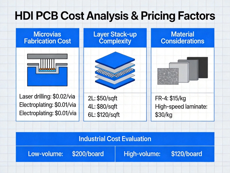
HDI boards typically cost 2 to 4 times more than equivalent standard multilayer boards due to increased process complexity, more manufacturing steps, and lower yields. However, the smaller board size and improved electrical performance can offset the higher per-area cost. The total system cost comparison must consider the benefits of Miniaturization, improved performance, and potential board count reduction.
How does via-in-pad affect assembly processes?
Via-in-pad requires special considerations during assembly. The filled and planarized via surface must provide a suitable soldering surface. Solder paste stencil design must account for the via location, and reflow profiles must accommodate any thermal differences between via-filled areas and solid copper. However, once these considerations are addressed, via-in-pad actually simplifies some assembly processes by eliminating the need to route vias away from component pads.
What design tools support HDI technology?
Most modern Pcb Design tools include HDI capabilities, but the quality and ease of use vary significantly. Key features to look for include Microvia definition, sequential lamination stackup definition, automatic via placement optimization, and impedance calculation for HDI structures. Some tools also provide 3D visualization that helps designers understand complex via structures and layer interactions.
HDI technology introduces specialized terminology that reflects its unique manufacturing processes and design considerations. Understanding this terminology enables engineers to communicate effectively with manufacturing partners, specify requirements accurately, and interpret technical feedback correctly. When designers and manufacturers share a common language, the collaborative process that produces successful HDI boards proceeds more smoothly.
The terminology covered in this glossary represents the core vocabulary needed for HDI design and manufacturing. As HDI technology continues evolving, new terms will emerge and existing terms may acquire refined meanings. Maintaining current knowledge of HDI terminology requires ongoing engagement with industry publications, standards updates, and manufacturer documentation.
Use this glossary as a reference when reviewing HDI specifications, discussing requirements with fabrication partners, or troubleshooting technical issues. Clear understanding of terminology prevents misunderstandings that can lead to costly design iterations or production problems. In the complex world of HDI technology, precise language becomes a competitive advantage.
Top 10 Frequently Asked Questions About HDI PCB TechnologyMay/28/2026
An Introduction to Microvia Technology in HDI PCBsJuly/24/2026
HDI PCB Cost Guide: What Factors Drive the Price Up?June/16/2026

Implementing a Robust Quality Control System for HDI ManufacturingJune/15/2026
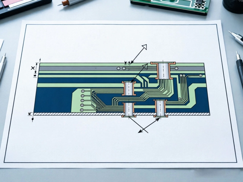
How to Read and Interpret HDI PCB Stack-up Drawings?July/14/2026
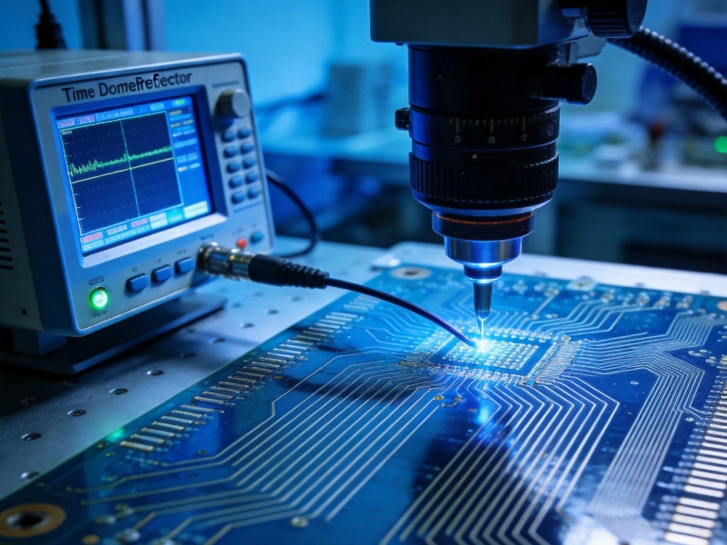
How to Measure and Control Impedance Tolerance in HDI BoardsAugust/03/2026
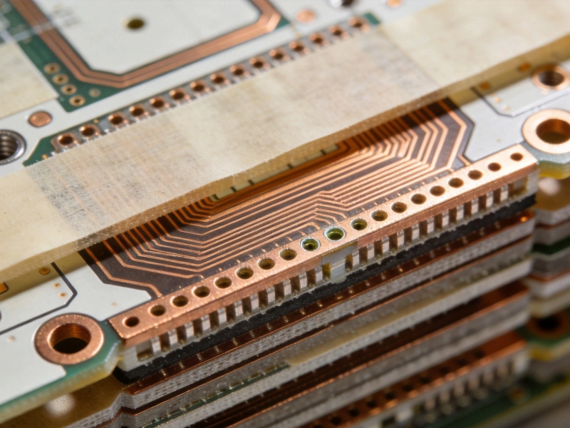
Exploring the 6 Types of HDI Structures: From Type I to Any-LayerAugust/14/2026
HDI Applications in Advanced Battery Management Systems (BMS)June/18/2026