Open Nav

Registration accuracy—the alignment between layers in a Multilayer Pcb—doesn't get much attention until it causes problems. And in HDI designs, it causes problems more often than in conventional multilayer boards. The combination of fine features, Microvias, and Sequential Lamination creates alignment tolerances that are tighter, more complex to control, and more consequential when they go wrong.
A misregistered layer in an HDI board can reduce annular rings below acceptable limits, break connections to Microvias, or create short circuits where misaligned features overlap. These aren't subtle failures—they're defects that render boards non-functional or unreliable. Understanding what affects registration, how to design for the reality of manufacturing tolerances, and how to verify alignment in production is essential for anyone designing High-density Interconnect boards.
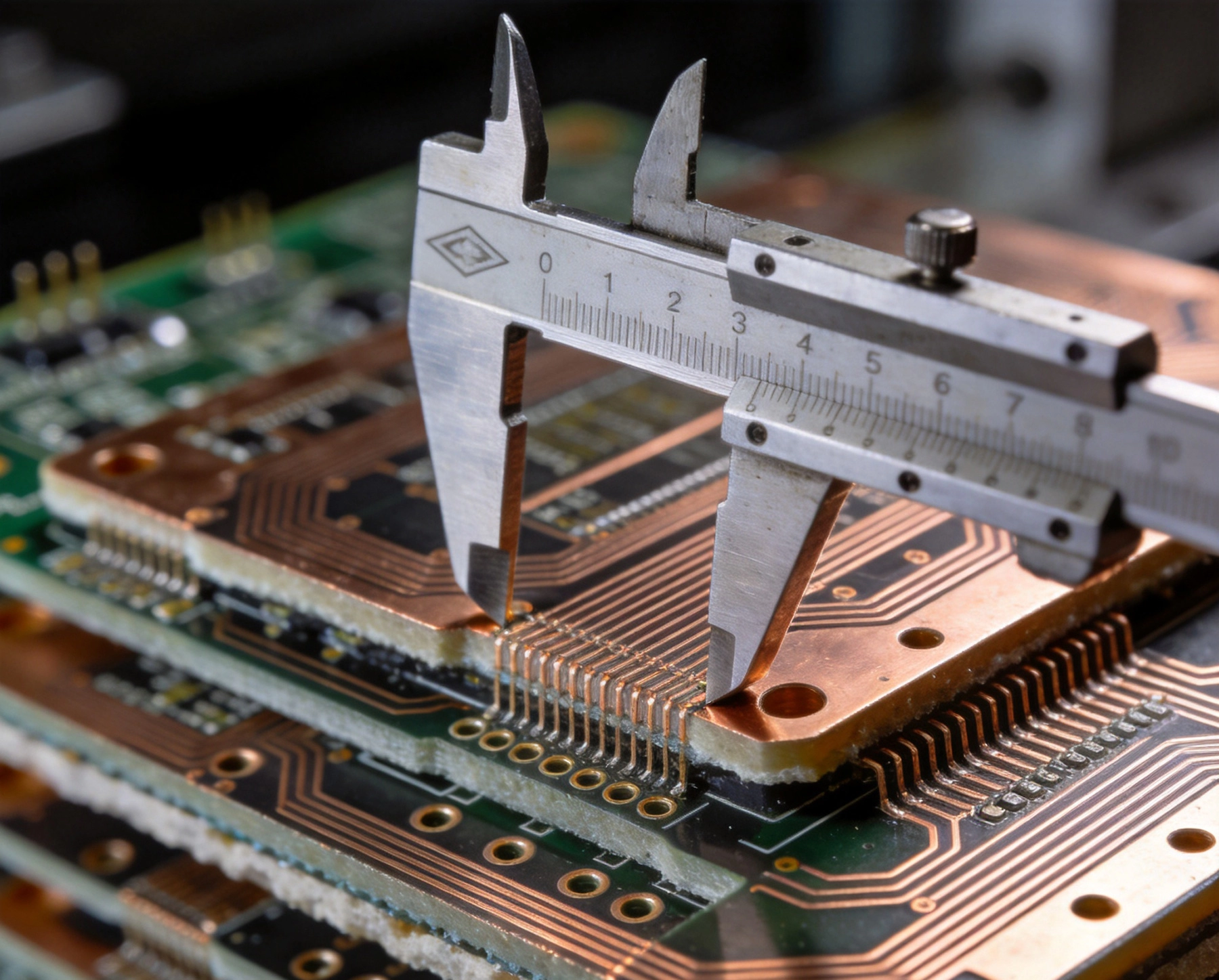
Registration accuracy describes how well features on different layers of a PCB align to their intended positions relative to each other. In a perfect board, every pad, trace, and via on every layer sits exactly where the design data specifies. In reality, every feature has some deviation from its nominal position, and the cumulative effect of these deviations determines whether the board functions correctly.
Registration is measured as the deviation between actual and nominal feature positions. This deviation has both systematic components (consistent shifts or scaling across a panel) and random components (feature-to-feature variation). Systematic errors can sometimes be compensated in process; random errors define the minimum annular ring you can reliably achieve.
For conventional multilayer boards with 8-mil traces and 20-mil vias, registration errors of a few mils are tolerable—the features are large enough that moderate misalignment doesn't cause problems. For Hdi Boards with 3-mil traces and 4-mil microvias, the same absolute error is catastrophic. The tolerance budget is smaller, and the manufacturing processes are more complex, creating more opportunities for error.
Registration errors come from multiple process steps, each contributing its own deviation:
The process of defining copper patterns on each layer starts with phototools or Laser Direct Imaging (LDI). Phototools—film negatives of the circuit pattern—can have dimensional instability from temperature and humidity changes during storage and handling. A film that stretches by 0.05% across a 18-inch panel creates a 9-mil registration error at the panel edges compared to the center.
LDI eliminates phototool film by projecting the pattern directly onto the photoresist with a laser. This removes film instability as an error source but introduces its own challenges—laser positioning accuracy, substrate flatness during exposure, and the calibration of the imaging system. For fine-pitch HDI work, LDI is generally preferred because it removes the largest source of imaging error.
During lamination, heat and pressure compress the prepreg and bond the layers together. This process causes dimensional movement in the inner layer cores. The copper on inner layers constrains the laminate locally—areas with heavy copper move less than areas with sparse copper. This differential movement, called foil shift, is a significant source of registration error in multilayer boards.
The magnitude of lamination movement depends on the material system, the copper distribution, the lamination press cycle, and the number of lamination steps. Standard FR-4 with typical processing might see 1 to 3 mils of movement. High-Tg materials or specialized low-CTE laminates can reduce this, but not eliminate it. The fabricator's process engineering—press temperature profiles, pressure ramps, and cooling rates—affects how much movement occurs and how predictable it is.
Drilled holes must align to the pad stack on each layer they connect to. The drill machine positions holes based on the drill file, but the actual hole position depends on the machine's positioning accuracy, drill bit wander, and the board's dimensional stability during the drilling process. Entry and backup material quality also affects drill accuracy.
For standard through-hole vias, the drilling typically happens after lamination, so the drilled position is relative to the already-laminated board. For microvias created by Laser Drilling, the positioning accuracy depends on the laser system's capabilities and the alignment method used. Laser-drilled microvias can achieve better positioning accuracy than mechanically drilled holes, but the process is different and must be controlled differently.
Hdi Boards built with Sequential Lamination—where the board is constructed in multiple lamination steps, with vias created between sub-composites at each step—face compounding registration challenges. Each lamination step introduces its own dimensional movement. The errors from each step accumulate, and the final registration depends on the sum of all steps' contributions.
A board built in three lamination steps has three opportunities for movement error. If each step contributes 1.5 mils of error, the cumulative effect might be 3 to 4 mils (not simply additive, because errors may partially cancel or compound depending on direction). This cumulative nature makes registration control in sequentially laminated HDI boards significantly more challenging than in single-lamination conventional boards.
You can't eliminate registration error, but you can design to accommodate it. The goal is ensuring that the board functions correctly within the manufacturer's achievable tolerance, not requiring zero error.
The annular ring—the copper pad area remaining around a drilled hole after accounting for drill wander and registration error—is the primary registration concern for through-hole vias. IPC standards define minimum annular rings based on the product's reliability class. The design must provide pad sizes large enough to maintain the minimum annular ring even at worst-case registration.
The calculation is straightforward: pad diameter minus drilled hole diameter, divided by two, minus the registration tolerance. If your pad is 24 mils, your drill is 12 mils, and your registration tolerance is 4 mils, your worst-case annular ring is (24-12)/2 - 4 = 2 mils. If IPC requires 2 mils minimum, you're right at the limit. If registration runs worse than expected, you fail.
For HDI designs with tight geometry constraints, the pad size needed for adequate annular ring may conflict with routing density requirements. This is a real trade-off—you either allocate more space for pads, accept a smaller annular ring with the associated reliability risk, or use via structures (like microvias) that avoid the through-hole registration problem entirely.
Teardrops—or fillets—add copper at the junction between a trace and a pad, widening the connection point. When registration error shifts a pad relative to its connecting trace, the teardrop provides additional copper that maintains the connection even with some misalignment. This is a simple, effective design technique that adds negligible routing impact but improves robustness to registration errors.
Most EDA tools support automatic teardrop generation. The teardrop parameters—length and width—should be set based on your expected registration tolerance and the feature sizes involved. For HDI boards with tight geometry, even small teardrops provide meaningful improvement in connection reliability.
Experienced fabricators apply scaling compensation to inner layer artwork to account for the dimensional movement they expect during lamination. If they know that a particular inner layer consistently shrinks by 1.5 mils across the panel during lamination, they scale the artwork slightly larger so that after shrinkage, the features land near their nominal positions.
This compensation requires process knowledge that comes from building many boards and measuring the actual movement. A fabricator who builds similar boards routinely has better compensation data than one encountering your design for the first time. This is one reason why using a fabricator experienced with your type of board improves registration outcomes—they have better scaling compensation data.
Several manufacturing process controls directly affect the registration accuracy you'll receive:
Larger panels experience more absolute registration error because dimensional changes scale with distance. A registration error of 0.02% across a 12-inch panel produces 2.4 mils of error; across an 18-inch panel, it's 3.6 mils. For HDI boards where every mil matters, smaller panel sizes provide better registration control at the cost of higher per-board fabrication cost (fewer boards per panel).
Feature distribution across the panel also matters. Uniform copper distribution minimizes differential movement during lamination. A board with heavy copper on one side and sparse copper on the other will move unevenly, creating registration challenges. The fabricator may recommend copper balancing—adding non-functional copper to sparse areas—to improve uniformity.
The laminate material's dimensional stability directly affects registration. Standard FR-4 (CTE of 14-18 ppm/°C in-plane) moves more during lamination than low-CTE materials designed for high-layer-count and Hdi Applications. Materials like IS410 or Megtron 6 offer better dimensional stability at a price premium.
For sequentially laminated HDI boards, the material choice is particularly important because the cumulative movement from multiple lamination steps amplifies any dimensional instability. The cost difference of a more stable material is often justified by the registration improvement and the yield increase it enables.
The lamination press cycle—temperature ramp rate, peak temperature, pressure profile, and cooling rate—affects how much dimensional movement occurs. Optimized press cycles for HDI boards typically use slower temperature ramps and controlled cooling to minimize thermal gradients that cause uneven movement. Your fabricator's press cycle engineering is a significant factor in registration outcomes.
Some advanced fabricators use multi-step press cycles with hold temperatures that allow the material to relax before reaching peak temperature. These cycles take longer but produce more predictable dimensional movement that's easier to compensate with scaling adjustments.
How do you know if your board actually achieved the registration accuracy you need? Verification happens at several points in the process:
First article inspection on the initial boards from a production run includes registration measurement. Cross-sectioning at Microvia locations reveals the actual alignment between layers. This destructive inspection is expensive but provides direct measurement of the most critical registration interfaces.
Non-destructive alternatives include electrical testing that verifies connectivity—if registration errors broke connections, electrical test catches them. However, electrical test doesn't measure marginal registration that didn't quite fail but may be unreliable. Cross-section provides the full picture.
Automated Optical Inspection systems can compare feature positions on exposed layers to design data, measuring the deviation from nominal. This provides statistical data on registration accuracy across the panel, identifying trends like scaling errors or systematic shifts that might not be apparent from individual measurements.
AOI registration data is particularly valuable during process development, when the fabricator is tuning scaling compensation for a new design. The statistical distribution of registration errors guides the compensation adjustments.
X-ray Inspection can reveal inner Layer Registration without destructive cross-sectioning. The resolution is limited compared to cross-section, but it provides a non-destructive check that's useful for monitoring production consistency. Significant registration deviations visible on X-ray warrant further investigation with cross-section.
Registration is a shared responsibility between design and manufacturing. The designer controls the tolerance budget—pad sizes, annular rings, and feature spacing. The fabricator controls the process—scaling compensation, press cycles, and material selection. The best outcomes come from collaboration.
Early engagement with your fabricator is the single most effective thing you can do to manage registration risk. Before you finalize your design, discuss: what registration tolerance they can realistically achieve for your board complexity, what pad sizes they recommend for your via types and reliability class, whether your copper distribution is balanced enough for good lamination results, and what material they recommend for your layer count and feature sizes.
Be skeptical of fabricators who claim unrealistic registration accuracy without supporting data. Ask what their measured registration capability is on boards similar to yours. Ask how they handle scaling compensation. Ask what happens when registration falls outside specification—do they scrap the board or try to recover it? The answers reveal whether they understand registration as a process to be managed or just a number to be claimed.
Typical production registration accuracy for a 12-layer HDI board is in the range of 3 to 5 mils, depending on the fabricator's capability, materials, and process controls. Advanced fabricators with optimized processes may achieve 2 to 3 mils. These are total registration tolerances that must be budgeted against annular ring requirements.
Sequential lamination compounds registration error because each lamination step introduces its own dimensional movement. A board built in three lamination steps has three opportunities for error accumulation. The cumulative effect typically means worse registration than a board of similar complexity built in a single lamination step.
Yes, LDI (Laser Direct Imaging) eliminates phototool film instability, which is often the largest single source of imaging registration error. For fine-feature HDI boards, LDI is generally recommended. The improvement is most significant for boards with features below 4 mils, where film instability becomes a substantial fraction of the feature size.
Specify your minimum annular ring requirement and let the fabricator determine the pad size needed to achieve it given their process capability. Alternatively, specify your design's maximum registration tolerance and ask the fabricator to confirm they can achieve it. The key is having a clear conversation about expectations before design completion.
Electrical testing detects registration errors that cause open or short circuits, but not marginal registration that might be unreliable. A via with a thin annular ring due to registration error might pass electrical test but fail under thermal cycling. Physical inspection (cross-section or X-ray) provides a more complete assessment of registration quality.
Contact us to discuss your requirements.
Selecting the Right Dielectric Materials for High-Performance HDI PCBsJune/05/2026
Understanding the Role of Copper Foil Roughness in Signal IntegritySeptember/23/2026
What is High Density Interconnect (HDI) PCB?May/28/2026

An Introduction to ABF (Ajinomoto Build-up Film) for Advanced HDIJuly/27/2026
Why Low Loss Materials are Critical for High-Speed HDI DesignsSeptember/01/2026
Essential HDI PCB Design Rules for Beginners and ExpertsMay/28/2026
FR-4 vs. High-Tg Materials: What Works Best for HDI Applications?July/07/2026
Precision in HDI FabricationJune/04/2026