
Signal Integrity engineers spend considerable effort on trace geometry, Impedance Control, and crosstalk management. Yet one factor often receives insufficient attention until problems emerge in production or field operation: copper foil surface roughness. At low frequencies, the microscopic texture of copper foil has negligible effect. But as signal speeds climb into the hundreds of megahertz and beyond, foil roughness becomes a dominant loss mechanism that can cripple system performance.
Understanding how copper foil characteristics affect signal propagation helps engineers make better material selections, communicate effectively with manufacturers, and troubleshoot problems when designs fail to meet performance targets. This knowledge proves increasingly valuable as data rates continue rising across telecommunications, computing, and automotive applications.
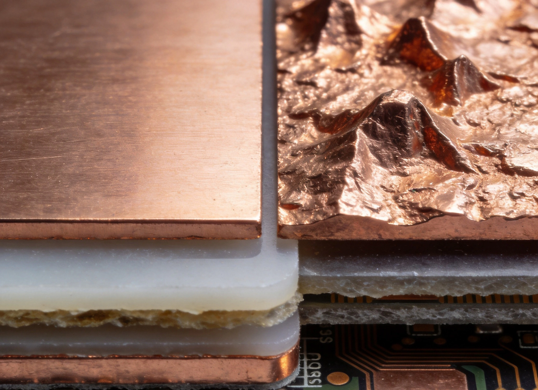
Copper foil used in PCB Fabrication is not perfectly smooth. The electrodeposition process that creates foil deposits copper in crystalline structures that form microscopic peaks and valleys. Standard electrodeposited (ED) foil exhibits roughness ranging from approximately 150 microinches (Ra) to over 300 microinches, measured as average peak-to-valley height across a sampling length.
The foil surface that bonds to substrate shows different characteristics than the foil surface exposed during processing. Foil manufacturers specify different roughness values for each side, with the treatment side typically rougher to improve bonding. This differential roughness affects how signals propagate depending on which surface faces the dielectric.
Surface roughness measurements include several parameters that describe different aspects of texture. Ra (arithmetic average) describes the average deviation from the centerline. Rz (maximum height) describes the average of the five tallest peaks plus five deepest valleys. Rp (maximum peak) and Rv (maximum valley) describe individual extremes. Each parameter provides different insight into how roughness affects electrical performance.
PCB designers typically specify roughness categories rather than numerical values. Standard foil roughness categories include STD (standard, typically 150-200 microinches Ra), Low-Profile (LP, typically 50-100 microinches Ra), and Very Low-Profile (VLP, typically 30-50 microinches Ra). Some high-performance applications specify ultra-smooth foil below 20 microinches Ra.
High-temperature-resistant foil (also called RTF or reverse treat foil) processes differently from standard foil, creating different surface characteristics. The bonding side of RTF foil is treated to create micro-roughness for adhesion while maintaining smoothness on the other side. This asymmetry provides both strong substrate bonding and reduced conductor loss on signal layers.
VLP-HTE foil combines very low profile on the signal-facing side with high-temperature resistance, providing the lowest loss option for demanding high-speed applications. These premium foils cost more than standard options but may be necessary when insertion loss budgets are tight.
At DC and low frequencies, current distributes uniformly across a conductor cross-section. As frequency increases, magnetic fields drive current toward the conductor surface, a phenomenon called skin effect. Skin depth, the depth at which current density falls to 1/e of its surface value, decreases with the square root of frequency. At 1 GHz, skin depth in copper is approximately 2 micrometers, meaning signals propagate primarily within the outermost copper layers.
Skin effect concentrates current in the region where roughness exerts maximum influence. If the rough surface profile penetrates to depths comparable to skin depth, the irregular surface effectively extends the signal path, increasing effective resistance and loss. This mechanism explains why roughness matters at high frequencies but has negligible effect at low frequencies.
When signal frequency means skin depth approaches or is smaller than surface roughness, the signal path no longer follows the smooth centerline of the conductor. Instead, current follows the jagged surface profile, lengthening the actual path the signal travels. This increased path length manifests as additional insertion loss that cannot be recovered through trace width or length adjustments.
The increased loss depends on both roughness magnitude and frequency. Roughness effects become measurable above several hundred megahertz and become severe at millimeter-wave frequencies. Designs targeting 25 Gbps per lane or higher face substantial loss from roughness unless explicitly specified.
Signal Integrity simulation tools incorporate roughness models that predict conductor loss from surface profile parameters. The Hammerstad model and similar approaches convert roughness measurements into effective conductivity reduction that increases loss. These models require accurate roughness inputs to produce reliable predictions.
Engineers using simulation should input measured roughness values rather than assuming nominal values. Manufacturing variation means actual roughness may differ significantly from nominal specifications, leading to simulation results that do not match measured performance.
High-speed serial links allocate total insertion loss budgets across multiple loss contributors: Dielectric Loss, conductor loss, vias, connectors, and surface roughness. As data rates increase, total budgets shrink while loss per bit remains roughly constant, meaning loss density increases. Roughness that represents 10% of loss at 5 Gbps may represent 30% or more at 25 Gbps.
Insertion loss budgets typically derive from channel specifications like IEEE 802.3 for Ethernet. These specifications set maximum channel loss at specific frequencies, forcing designers to minimize all loss contributors. Ignoring roughness in budget allocation leads to designs that fail compliance testing.
Signal loss narrows eye diagrams by attenuating high-frequency components that define signal transitions. Slower transitions increase timing jitter as signals take longer to cross voltage thresholds. While Dielectric Loss contributes to this effect, conductor loss from roughness does as well, and both must be addressed when closing timing budgets.
Jitter budgets allocate portions to various contributors including intersymbol interference from loss. Roughness-induced loss creates deterministic jitter that repeats pattern-to-pattern, distinguishing it from random jitter from noise sources. Understanding jitter components helps isolate roughness-related problems.
Surface roughness affects impedance through its effect on effective conductor geometry. The irregular surface creates slight impedance variations along the trace length, causing reflections and degrading return loss. While these variations are typically small, they compound at high frequencies where even minor imperfections matter.
Return loss specifications for high-speed interfaces like PCIe and Ethernet quantify acceptable reflection levels. Designs exceeding return loss limits may fail to interoperate with other equipment or may experience data errors in noisy environments.
Application requirements drive appropriate foil selection. For digital logic at frequencies below 100 MHz, standard foil roughness causes negligible signal degradation. Cost-conscious designs for these applications should not pay premium pricing for low-profile foil that provides no measurable benefit.
As frequencies rise into the hundreds of megahertz and low gigahertz range, roughness effects become noticeable. Server, telecommunications, and networking equipment operating above 5 Gbps typically specifies low-profile or very low-profile foil to maintain signal integrity margins. Automotive applications including autonomous driving sensors increasingly require premium foil for radar and high-speed data links.
Digital standards continue pushing data rates higher. PCIe Gen 4 at 16 GT/s and Gen 5 at 32 GT/s create challenging loss budgets that demand attention to every contributor. Serial differential pairs at these rates may be the most loss-sensitive portions of the system, with roughness potentially accounting for 20-30% of total loss.
Network switches, routers, and optical transport equipment operate at similar or higher rates, requiring the same attention to foil selection. These applications often specify VLP-HTE foil to ensure adequate margins.
Radio frequency and microwave applications face even more stringent requirements as wavelengths shrink and frequencies climb. At 77 GHz automotive radar frequencies, skin depth is approximately 0.75 micrometers, meaning virtually all current flows within the roughest portion of the conductor surface. Conductor loss dominates over dielectric loss at these frequencies.
RF applications often specify investment-cast or rolled copper that offers smoother surfaces than standard electrodeposited foil. Rolled copper provides roughness below 10 microinches Ra, dramatically reducing conductor loss. These premium materials enable feasible designs at frequencies where standard foil would be impractical.
Smoother copper foil presents a bonding challenge. The rough surface that reduces signal loss also provides mechanical adhesion to substrate materials. Ultra-smooth foil may require specialized bonding treatments or alternative prepreg systems to achieve reliable lamination without delamination risk.
Material suppliers have developed low-profile foil with optimized surface treatment that balances loss reduction with bonding performance. These products provide significant loss improvement over standard foil while maintaining acceptable adhesion. Evaluate specific products against your bonding and reliability requirements.
When designing multilayer boards with high-speed signals, consider which layer contains the critical traces and which side of the foil carries the signal. Placing signal traces against the smoother foil side (typically the secondary treatment side) reduces loss compared to traces on the rough bonding side. This positioning may require different reference plane arrangements than typical designs.
For differential pairs, ensure both conductors in a pair use the same foil treatment and positioning to maintain symmetry. Asymmetric treatment between pair members causes mismatched loss that degrades common-mode performance.
Roughness increases effective conductor width for loss calculations. A trace with 150 microinch roughness on a 5-mil wide conductor may effectively be 10-15% wider for high-frequency current distribution. This effect slightly reduces impedance from nominal calculations, potentially requiring narrower traces to hit impedance targets.
Signal integrity simulation should include measured or estimated roughness in the model. Design rule checking should account for roughness effects on impedance when tolerance budgets are tight.
Return path quality matters as much as signal path quality. If the reference plane uses rough foil while the signal trace uses smooth foil, return current on the plane still experiences roughness loss. For minimum total loss, consider foil treatment on reference planes as well as signal traces.
Some designs place high-speed signals between smooth-foil inner layers, with reference planes also using smooth foil. This approach maximizes loss reduction but increases material and manufacturing complexity.
Include foil roughness specifications in your design documentation and manufacturing requirements. Specify nominal profile type (STD, LP, VLP) or request specific roughness measurements. When loss budgets are tight, consider requiring roughness testing certificates with each order.
PCB manufacturers purchase foil from suppliers and may not control roughness directly. Specify requirements clearly and discuss feasibility with potential manufacturers early in the design process. Some manufacturers stock limited foil types while others can source specific products.
Copper foil roughness is not perfectly consistent within a lot, between lots, or between manufacturers. Even foil labeled as VLP may vary from 30 to 50 microinches Ra depending on manufacturing conditions. This variation affects signal loss and may explain performance differences between prototype and production units.
For tight loss budgets, consider qualifying specific foil lots and requesting that manufacturing use those lots for your boards. This approach reduces variability but may increase cost and lead time.
Measure actual roughness using profilometry or optical methods to verify specifications match requirements. Roughness testing of production samples confirms that delivered boards meet roughness assumptions in signal integrity models. Discrepancies between expected and measured roughness explain many otherwise puzzling performance variations.
Time-domain reflectometry (Tdr) can detect effective loss differences that roughness causes. While Tdr alone cannot separate roughness effects from other loss contributors, comparisons between boards with known roughness differences reveal the impact.
Low-profile and very low-profile foil costs significantly more than standard foil. VLP-HTE foil may cost two to three times standard foil per square foot. For large boards with extensive high-speed routing, material cost differences may be substantial.
Evaluate whether performance requirements justify premium material costs. If a design fails loss budgets without low-profile foil, the additional material cost may be necessary. If budgets have substantial margin, standard foil may work without incident.
Premium foil products have longer lead times and potentially limited availability compared to standard foil. During periods of high demand for data center or networking equipment, VLP-HTE foil supplies tighten. Plan material procurement accordingly for designs requiring premium foil.
Some manufacturers maintain inventory of common foil types while sourcing others on demand. Lead time impacts of specific material selections should factor into project scheduling.
Roughness effects become measurable above approximately 500 MHz for standard foil. However, the threshold depends on specific roughness magnitude and loss budget constraints. Sensitive measurements detect roughness effects starting around 100-200 MHz, while practical designs may not notice impacts until several gigahertz.
Compared to standard foil, low-profile foil typically reduces conductor loss by 20-30% at 10 GHz. Very low-profile foil may reduce loss by 40-50%. These improvements come with corresponding cost increases, so evaluate whether budget margins justify premium materials.
PCIe Gen 5 at 32 GT/s creates challenging loss budgets that may be impossible to meet with standard foil. However, feasibility depends on channel length, connector counts, and other factors. Simulate with actual roughness assumptions to determine whether standard foil works for your specific design.
Differential pairs experience similar roughness effects on each conductor. However, if the two conductors of a pair use different foil treatments or if treatment varies along their length, differential-to-common-mode conversion may increase. Maintain consistent treatment across pair length for best performance.
Profilometry provides direct measurement by drawing a stylus across the surface. Optical methods like confocal microscopy or interferometry offer non-destructive alternatives. Request roughness testing from your manufacturer or use laboratory services to verify foil characteristics.
Copper foil roughness represents a critical but often overlooked factor in High-speed Pcb design. As data rates continue climbing, the impact of roughness on signal integrity grows proportionally. Engineers who understand and account for roughness effects early in design avoid costly surprises during testing and production.
Material selection should follow from system requirements rather than defaulting to familiar choices. Evaluate loss budgets against available foil options, specify requirements clearly to manufacturers, and verify performance through testing. This systematic approach ensures designs meet performance targets while controlling costs appropriately.
Essential HDI PCB Design Rules for Beginners and ExpertsMay/28/2026
Why Low Loss Materials are Critical for High-Speed HDI DesignsSeptember/01/2026
Managing Layer-to-Layer Registration Accuracy in Multilayer HDIOctober/09/2026
An Introduction to ABF (Ajinomoto Build-up Film) for Advanced HDIJuly/27/2026
What is High Density Interconnect (HDI) PCB?May/28/2026
FR-4 vs. High-Tg Materials: What Works Best for HDI Applications?July/07/2026
Selecting the Right Dielectric Materials for High-Performance HDI PCBsJune/05/2026
The Role of Thermal Vias in Dissipating Heat from HDI BoardsJune/09/2026