Open Nav

The computing industry stands at another bandwidth inflection point. PCIe Gen5 doubled per-lane data rates to 32 GT/s compared to Gen4, and PCIe Gen6 pushes further to 64 GT/s. These increases sound incremental on paper, but the engineering challenges they create are anything but. At 32 GT/s and beyond, the humble printed circuit board transforms from passive infrastructure into the critical enabler—or limiting factor—for system performance. HDI (High-density Interconnect) technology has emerged as the essential manufacturing approach for servers, accelerators, and networking equipment that must operate at these speeds reliably.
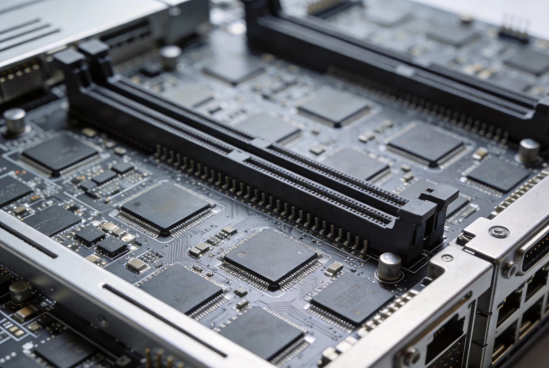
Understanding why Hdi Technology has become indispensable for PCIe Gen5 and Gen6 requires examining Signal Integrity physics, package-to-board interconnection challenges, and the manufacturing capabilities that enable reliable high-speed operation. This article explores the technical intersection of Hdi Manufacturing and next-generation computing interconnects.
PCIe Gen4 delivered 16 GT/s per lane, enabling x16 slots to move 64 GB/s in each direction. That bandwidth seemed adequate for emerging accelerators like GPUs and FPGAs when the specification released in 2017. By 2024, the demands of AI training, inference acceleration, and high-performance storage changed those calculations entirely.
PCIe Gen5 doubled the per-lane rate to 32 GT/s, instantly creating x16 slots capable of 128 GB/s bidirectional throughput. This doubling arrives as compute密度 increases faster than ever—AI accelerators now sport memory bandwidths exceeding 2 TB/s, requiring faster pathways to CPU and between accelerators. Gen5 provides the headroom these systems need.
The engineering challenge lies in achieving reliable 32 GT/s signaling over the distances involved in server and networking equipment. Signal Integrity degrades with frequency, and the tolerances that worked at Gen4 speeds become inadequate. Hdi Technology addresses these challenges through improved controlled impedance, reduced layer counts for critical paths, and better electrical performance.
PCIe Gen6 represents a more fundamental change by adopting PAM4 (Pulse Amplitude Modulation) signaling. Where previous PCIe generations used NRZ (Non-Return-to-Zero) with two signal levels, PAM4 uses four levels, effectively doubling the bits transmitted per symbol. This approach achieves 64 GT/s per lane but introduces new signal integrity complexities.
PAM4 reduces voltage margin compared to NRZ, making the system more sensitive to noise, ISI (Inter-Symbol Interference), and channel loss. The eye opening for PAM4 is substantially smaller than Gen5, requiring more sophisticated equalization, tighter manufacturing tolerances, and improved substrate materials. HDI technology provides the foundation for meeting these demanding requirements.
The transition to PAM4 affects both the die-level SerDes design and the PCB-level interconnection. Package substrates, motherboards, and riser cards all require optimization for PAM4 signaling. Hdi Manufacturing capabilities directly enable the channel performance these systems require.
Standard multilayer PCBs use through-hole vias that penetrate entire board stacks. When signals propagate along these vias, the untestubbed portion below the signal layer acts as a resonant stub, causing frequency-dependent loss and reflection. At PCIe Gen4 speeds, these effects required careful management; at Gen5 and Gen6 speeds, they become catastrophic without mitigation.
Blind and Buried Vias eliminate the stub problem by connecting only the layers that carry signals. A Blind Via from layer 1 to layer 4 has no stub below layer 4, eliminating the resonant behavior. HDI manufacturing enables these structured via approaches that are fundamental to high-speed operation.
The stub resonance frequency depends on stub length and dielectric properties. As signal speeds increase, the maximum allowable stub length decreases proportionally. Gen5 and Gen6 channels require stub lengths measured in tens of mils rather than hundreds, necessitating Blind Via technology.
Standard Pcb Manufacturing uses pads sized for reliable plating and assembly. These pad dimensions consume routing space and create capacitive loading that affects high-speed signals. At 32 GT/s and beyond, pad parasitic capacitance influences impedance matching and signal quality.
HDI technology achieves smaller pad sizes through advanced imaging and plating processes. Microvia diameters of 0.1mm to 0.15mm replace standard vias, dramatically reducing pad capacitance. The reduced pad geometry enables tighter routing density while improving high-frequency electrical performance.
Smaller annular rings—the copper ring around via holes—further reduce pad size and parasitic effects. Standard Annular Ring tolerances of 0.2mm or more become excessive for Gen5/Gen6 applications. HDI processes achieve annular rings below 0.1mm reliably, enabling the pad geometries these speeds require.
Multilayer PCBs build up layer by layer, with each layer requiring precise alignment to previous layers. Standard tolerance of 0.1mm to 0.15mm layer-to-Layer Registration may be acceptable for Gen4 channels, but Gen5 and Gen6 require tighter control to maintain signal integrity.
HDI manufacturing employs specialized lamination and imaging processes that achieve registration tolerances of 0.05mm or better. This precision ensures that Blind Vias connect to the correct traces on underlying layers, maintaining the controlled impedance paths that high-speed signaling demands.
Registration accuracy affects not just electrical performance but also yield. Misaligned Blind Vias may create opens or high-resistance connections that fail testing. The improved process control of HDI manufacturing reduces these defects, improving both performance and reliability.
HDI PCBs construct layer stacks sequentially rather than drilling all holes through the full board thickness. This approach allows each layer pair to be built with appropriate features before adding subsequent layers. The result is a structured board architecture with defined electrical paths optimized for high-speed operation.
Sequential buildup typically starts with a core substrate, then adds buildup layers on one or both sides. Each buildup cycle includes dielectric lamination, Microvia formation, copper deposition, and pattern plating. The number of buildup cycles determines total layer count and affects manufacturing cost and cycle time.
For PCIe Gen5 and Gen6 applications, this sequential approach allows placement of critical high-speed layers adjacent to reference planes, minimizing loop inductance and controlling impedance precisely. The flexibility to position signal layers optimally distinguishes HDI from standard processes.
Microvia formation uses Laser Drilling rather than mechanical drilling for holes smaller than approximately 0.15mm. Laser Drilling achieves smaller diameters, better positional accuracy, and faster throughput than mechanical drilling for fine features. These capabilities enable the microvia densities that HDI requires.
CO2 lasers machine the Dielectric Material in organic boards, while UV lasers provide finer control for sensitive applications. The laser parameters—pulse energy, repetition rate, and focus position—require optimization for different materials and via geometries. This process knowledge separates experienced HDI manufacturers from those learning the technology.
Microvia aspect ratio—depth to diameter—affects plating difficulty and reliability. HDI processes typically maintain aspect ratios below 1:1 for reliable filling, requiring careful stackup design. The depth constraints of Microvia Technology influence overall board thickness and layer distribution.
The most advanced HDI structures—Any-layer Hdi—allow blind and Buried Vias to connect any combination of internal layers. This maximum flexibility enables optimization of high-speed routing paths, allowing signals to traverse the board using the most efficient routes without unnecessary layer changes.
Any-layer Hdi achieves the ultimate in routing optimization but at premium cost and manufacturing complexity. Not all applications require this capability; simpler HDI structures may provide adequate performance at lower cost. Understanding the actual requirements helps specify the right HDI complexity.
Package-on-package stacking and complex IC substrates sometimes use any-layer HDI principles to achieve the interconnection density they require. The techniques developed for PCB-level any-layer HDI translate to substrate manufacturing, blurring the boundaries between packaging and board-level interconnection.
PCIe specifications define nominal impedance and tolerance for channels. Gen5 maintained the 85 ohm Differential Impedance standard, but achieving and maintaining this impedance through the channel requires manufacturing precision that standard processes cannot reliably deliver.
Impedance depends on trace geometry (width and thickness), dielectric properties, and proximity to reference planes. HDI processes provide tighter control over all these variables—trace width variation remains within tighter tolerances, dielectric constant variation is minimized, and layer-to-layer spacing is controlled precisely.
Tolerance allocation for impedance becomes tighter at higher speeds. Where Gen4 might allow 10% impedance variation, Gen5 typically requires 7-8%, and Gen6 may tighten further. HDI manufacturing provides the process capability to achieve these demanding tolerances consistently.
Modern SerDes implementations include sophisticated equalization to compensate for channel loss and dispersion. CTLE (Continuous Time Linear Equalization), DFE (Decision Feedback Equalization), and FFE (Feed Forward Equalization) work together to open receive-side eyes degraded by the channel. However, equalization has limits—channels exceeding loss budgets cannot be rescued by additional equalization.
HDI technology reduces channel loss compared to standard constructions. Lower-loss dielectrics, reduced pad capacitance, and controlled impedance paths all contribute to lower Insertion Loss per inch. For long channels typical of server motherboards and backplanes, these loss reductions matter significantly.
The interaction between channel design and equalization settings requires co-design across system, package, and board domains. System architects must balance equalization capability against channel loss to achieve reliable operation at target bit rates and distances.
PCIe specifications define maximum channel loss that compliant systems must support. Gen5 specified 36 dB loss at Nyquist frequency for x16 channels, with options for shorter channels supporting higher speeds. Gen6 tightens these budgets further due to PAM4 sensitivity.
Loss budget allocation across the channel includes contributions from traces, vias, connectors, packages, and any other discontinuities. HDI technology reduces the via and trace contributions, leaving more margin for other elements or enabling longer total channel length.
Material selection affects loss significantly. Standard FR-4 materials exhibit higher loss at Gen5 and Gen6 frequencies than low-loss alternatives. Combined with HDI construction, Low-loss Materials enable channels that meet demanding loss budgets while maintaining manufacturing practicality.
PCIe accelerators and high-speed processors consume substantial power—200W to 700W per device is common in AI training systems. This power dissipates as heat through the PCB substrate, creating thermal gradients that affect both reliability and electrical performance. HDI constructions must manage this thermal challenge.
Thermal Vias conduct heat away from high-power devices through the board stack. HDI microvia arrays provide high Thermal Conductivity paths when properly designed. The density of Thermal Management structures competes with routing density, requiring careful optimization for combined thermal and electrical requirements.
High-speed channel performance degrades with temperature due to material property changes. Maintaining stable temperature across operating ranges ensures consistent signal integrity. Thermal Management design must consider both absolute temperature and temperature gradients across critical signal paths.
Data center equipment operates continuously for years, experiencing thermal cycles from load variations and environmental changes. The dielectric materials, copper traces, and via structures must survive thousands of thermal cycles without degradation that affects electrical performance.
HDI constructions with Microvias face different reliability challenges than through-hole vias. Microvia Reliability depends on plating quality, interface adhesion, and stress concentration at geometry transitions. Experienced manufacturers understand the process controls that ensure Microvia Reliability in demanding applications.
Accelerated life testing validates reliability assumptions before deployment. Temperature cycling, thermal shock, and power cycling tests reveal failure mechanisms that may not appear in initial testing. Qualification programs for data center equipment include these stress tests to ensure field reliability.
Conductive Anodic Filament (CAF) formation—the growth of copper filaments through dielectric under bias voltage—causes failures that may appear after months or years of operation. HDI constructions with fine geometries and controlled dielectric properties reduce CAF susceptibility compared to standard constructions.
Material selection affects CAF resistance significantly. High-Tg materials, CAF-resistant dielectrics, and careful processing all contribute to resistance. For data center applications requiring long life, specifying CAF-resistant materials and processes provides insurance against these latent failures.
HDI manufacturing requires superior imaging resolution compared to standard PCB processes. Trace widths below 75 microns, spacing below 75 microns, and registration below 50 microns demand Laser Direct Imaging (LDI) rather than traditional photographic imaging. LDI systems provide the resolution and positional accuracy that HDI requires.
Panel size limitations may apply for advanced HDI processes. Some manufacturers image and plate individual boards rather than panels, trading throughput for capability. Understanding manufacturer limitations helps specify achievable geometries.
Line quality—edge sharpness, uniformity, and defect density—affects both electrical performance and manufacturing yield. HDI processes optimized for high-speed applications achieve better line quality than processes focused on cost reduction.
Microvia Filling and Via-in-pad plating require sophisticated electrolytic and electroless copper processes. Panel plating must achieve uniform thickness across large areas while also filling microvia features. This combination challenges standard plating approaches, requiring modified processes or specialized equipment.
Via-in-pad construction—where component pads contain the via barrel—eliminates antipads and improves routing density but requires void-free plating fill. Void-containing fills create reliability risks and affect high-frequency performance. Manufacturers must demonstrate reliable void-free filling capability.
Copper purity and grain structure affect conductivity and migration resistance. High-purity copper with controlled grain orientation provides better electrical performance and long-term reliability. Material specifications should address these quality attributes.
Electrical testing for high-speed PCBs extends beyond simple continuity testing. Time-domain reflectometry (Tdr) identifies impedance discontinuities; vector network analysis (VNA) measures S-parameters across frequency ranges. These tests validate that manufactured boards meet the electrical requirements that specifications demand.
PCB Fabrication documentation should include electrical test results demonstrating compliance with impedance and loss requirements. Flying probe testers, coupon structures, and cross-section analysis all contribute to verification. Understanding which tests provide confidence for your application helps specify appropriate requirements.
First-article inspection for new designs validates manufacturing process capability before production commitment. Cross-sections revealing via structure, plating thickness, and dielectric properties confirm that processes achieved intended geometries. This qualification investment prevents production problems.
Not all PCB manufacturers claiming HDI capability can achieve the tolerances required for PCIe Gen5 and Gen6. Capability verification through audit, sample evaluation, and qualification testing provides evidence that manufacturers can deliver required performance.
Requesting actual cross-section data from previous high-speed projects demonstrates manufacturing process capability. Well-documented processes, statistical process control, and capability indices (Cpk) quantify manufacturing consistency. Manufacturers should be able to provide evidence of their process capability.
On-site audits allow direct observation of equipment condition, process controls, and personnel competence. For critical applications, supplier qualification programs include audit requirements that verify capability claims through direct observation.
High-speed Pcb performance depends on material properties that vary between laminate types and even between lots of the same material. Specifying qualified materials and lot-to-lot consistency requirements helps ensure predictable performance from board to board.
Low-loss Materials from qualified suppliers provide the property consistency that Gen5 and Gen6 require. Material datasheets specify nominal values, but actual lot variation may affect electrical performance. Working with manufacturers who qualify specific material lots provides tighter control.
New material introductions require qualification time and cost. For applications with long lifecycles, material continuity planning helps avoid requalification expenses when materials become obsolete or unavailable. Manufacturers with broad material relationships can help navigate these transitions.
Data center equipment often enjoys multi-year lifecycles, requiring consistent PCB supply across extended periods. Partnering with manufacturers who understand these continuity requirements helps ensure supply stability across product life.
Engineering support capabilities matter for complex high-speed designs. Manufacturers who contribute design feedback, DFM recommendations, and failure analysis provide value beyond manufacturing capability. These contributions improve first-pass success and accelerate problem resolution.
Geographic proximity affects logistics, communication, and response time for urgent needs. Whether domestic or offshore manufacturing best fits your situation depends on volume, timeline, and support requirements. The total cost comparison should include logistics and risk factors, not just unit pricing.
The computing industry already plans beyond current PCIe generations. While Gen7 specifications remain under development, the trend toward higher data rates continues. HDI technology will need to evolve further to support these future requirements—smaller features, better materials, and more sophisticated manufacturing.
Optical interconnection may eventually supplement or replace electrical PCIe at very high speeds, but this transition remains years away for most applications. Electrical channels will continue serving the majority of interconnection needs, requiring ongoing HDI capability advancement.
The boundary between PCB and package continues to blur as integration density increases. Embedded die, Chiplet architectures, and substrate-level interconnection extend HDI principles into packaging domains. Understanding these trends helps plan long-term technology roadmaps.
Co-design across package and PCB domains becomes increasingly important as signals traverse multiple interconnection boundaries. System architects must consider the combined channel from die to die, across package substrates, through PCB to other modules. HDI expertise spans these boundaries in organizations that understand both packaging and board-level interconnection.
Materials evolution continues addressing the loss and stability challenges of high-speed operation. Ultra-low-loss dielectrics, glass substrates, and advanced copper treatments all contribute to improved high-frequency performance. Staying current with material development enables access to improved capabilities.
Manufacturing process innovation similarly advances what is achievable. Improved laser systems, advanced plating chemistries, and better process controls push HDI capabilities forward. Partners investing in process R&D provide access to capabilities before they become standard offerings.
PCIe Gen5 typically requires at least sequential build-up HDI with laser-drilled Microvias. The specific layer count and via structure depend on channel length, loss budget, and package type. Minimum requirements generally include blind microvias with proper stub management and controlled impedance on critical layers.
Properly manufactured microvias demonstrate excellent reliability, often exceeding through-hole via performance under thermal cycling. However, microvia reliability depends critically on manufacturing quality—voids, plating discontinuities, or interface weaknesses cause failures. Working with qualified manufacturers ensures reliable microvia performance.
HDI PCBs typically cost 30-100% more than equivalent standard multilayer boards, depending on complexity and layer count. For PCIe Gen5 applications, this premium is justified by the performance requirements that standard boards cannot meet. The cost difference narrows at higher volumes as setup costs amortize.
Low-loss materials with stable dielectric properties at high frequencies suit PCIe Gen5 and Gen6 applications. Examples include Panasonic Megtron 6, Isola I-Tera, Rogers RO4000 series, and similar products. Material selection depends on specific loss budgets, thermal requirements, and manufacturing compatibility.
Only manufacturers with demonstrated HDI capability and appropriate process controls can reliably produce PCIe Gen5 boards. Most standard manufacturers lack the equipment, process knowledge, or quality systems for these demanding applications. Capability verification through audit or sample evaluation is essential before supplier selection.
PCIe Gen5 and Gen6 computing requirements have fundamentally changed what Pcb Manufacturing must deliver. The signal integrity demands of 32 GT/s and 64 GT/s signaling cannot be met by standard PCB processes—HDI technology has become essential infrastructure for data center, networking, and high-performance computing applications.
Understanding the technical requirements—stub management, controlled impedance, loss budgets, and manufacturing tolerances—provides the foundation for specifying appropriate HDI capabilities. The partnership between system designers and PCB manufacturers becomes increasingly important as speeds increase and tolerances tighten.
Organizations investing in HDI manufacturing capability position themselves to address not just current PCIe generations but the higher speeds and integration densities that future computing demands. The technology investment required is substantial, but the market opportunity in AI, cloud computing, and high-performance data center applications rewards those who can deliver.
HDI technology will continue evolving alongside computing requirements. The engineering teams and manufacturing partners who understand this evolution will lead in serving the demanding applications that next-generation computing enables.

The Role of HDI in High-Speed Server and Data Center HardwareJuly/18/2026
Signal Integrity Challenges in 5G mmWave HDI DesignsAugust/08/2026
Enabling 5G Base Stations with Low-Loss HDI PCB MaterialsJune/27/2026
HDI Solutions for High-Performance Gaming Consoles and LaptopsSeptember/10/2026
The Impact of Plating Voids on HDI Interconnect ReliabilityJuly/10/2026

Implementing a Robust Quality Control System for HDI ManufacturingJune/15/2026
Copper Coin and Embedded Heat Sinks: Advanced Cooling for HDIJuly/08/2026
How X-Ray Inspection (AXI) Detects Hidden Defects in HDI BoardsJuly/30/2026