
Modern electronic devices demand ever-increasing functionality packed into shrinking form factors. This relentless Miniaturization drives the adoption of High-density Interconnect (HDI) printed circuit board technologies, where Microvias serve as the critical interconnections enabling complex routing in space-constrained designs. However, these microscopic features face a formidable challenge: the thermal cycling inherent to electronic device operation. Microvia cracking during thermal cycling has emerged as one of the most significant reliability concerns in advanced electronic assemblies, capable of causing intermittent failures, complete circuit opens, and costly field returns.
Understanding the mechanisms behind Microvia cracking, and implementing effective prevention strategies, has become essential knowledge for engineers designing reliable electronics for automotive, aerospace, telecommunications, and consumer applications. This comprehensive guide examines the physics of thermal stress in Microvias, identifies the factors contributing to crack formation, and provides actionable design and manufacturing practices to ensure long-term reliability.
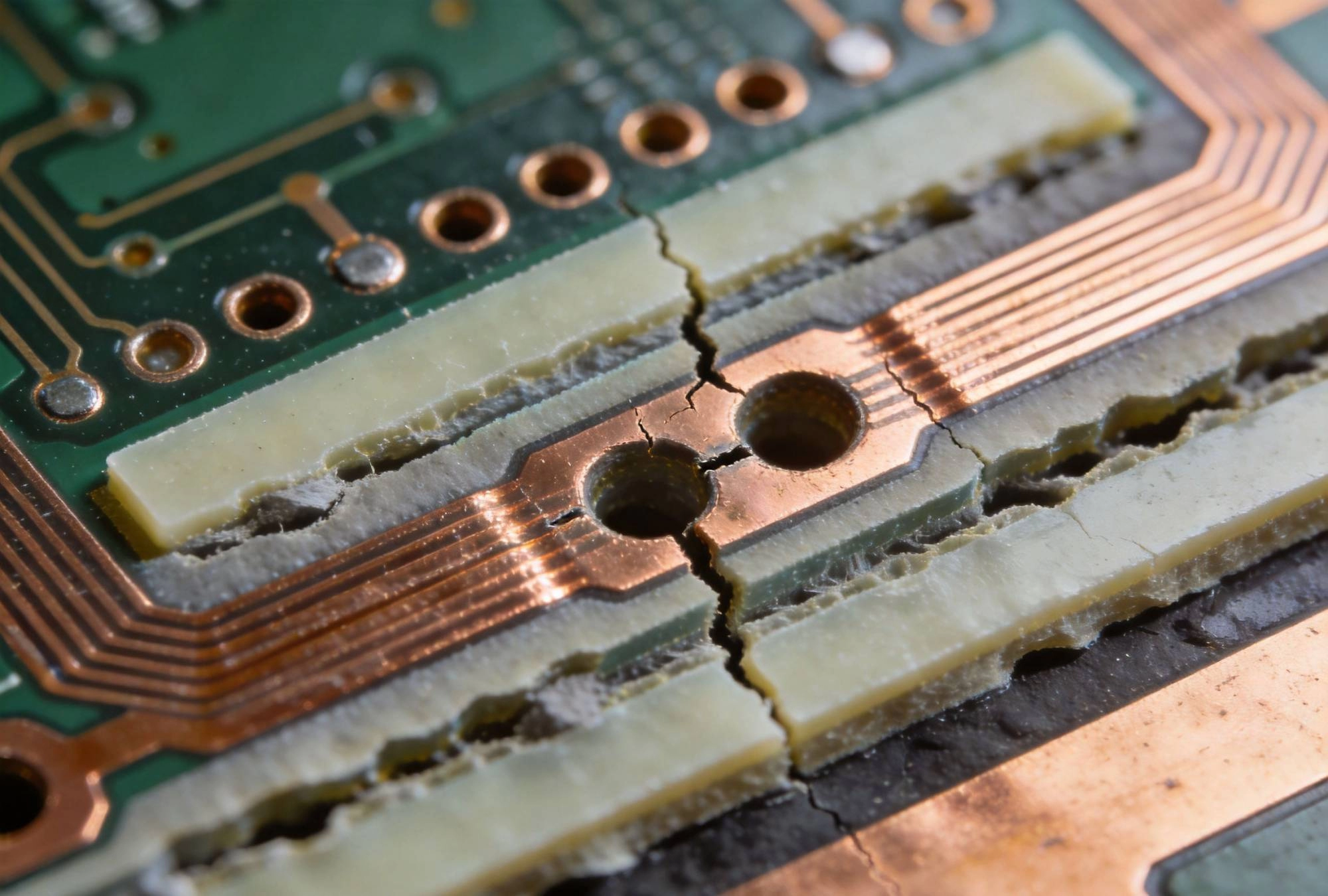
To understand microvia cracking, we must first grasp the fundamental physics governing material behavior during temperature changes. Microvias exist in an environment of competing thermal expansion forces that create cyclic stress on the small but critical interconnect structures.
The root cause of thermal cycling damage lies in the mismatch between coefficients of thermal expansion (CTE) among the different materials comprising a microvia structure. A typical HDI board stackup includes copper metallization, dielectric laminates, prepreg bonding layers, and potentially solder mask coatings. Each material exhibits its own characteristic CTE, measured in parts per million per degree Celsius (ppm/°C).
Consider the most common Cte Mismatch scenario: copper foil has a CTE of approximately 17 ppm/°C, while the Z-axis CTE of standard FR-4 laminate ranges from 50 to 70 ppm/°C. During thermal cycling, when the assembly temperature changes from room temperature to an elevated operating temperature, the laminate wants to expand three to four times more than the copper barrel of the microvia. This differential expansion creates shear stresses at the copper-dielectric interface, with the greatest stress concentration occurring at the top and bottom of the via barrel where the constraint is most severe.
As the assembly cools, the process reverses: the laminate contracts more aggressively than the copper, creating tensile stresses that pull at the interface. Each complete thermal cycle places the microvia under this cyclic loading pattern, gradually accumulating damage with each repetition.
Microvias represent dramatic geometrical discontinuities in the Dielectric Material. The sharp corners at the top of the via barrel, the transition between the Blind Via and the underlying plane, and any irregularities in the plated copper all act as stress concentration points. According to classical fracture mechanics, sharp corners can amplify applied stress by factors of two to five, making these locations the most vulnerable to crack initiation.
The fatigue life of a microvia depends not only on the magnitude of cyclic stress but also on stress concentration at these geometric features. Improving the smoothness of transitions and eliminating sharp corners in via geometry significantly reduces stress concentration factors, extending the number of cycles to failure.
Microvia failure under thermal cycling follows a predictable progression through distinct phases, each characterized by specific physical mechanisms and observable symptoms. Understanding this evolution helps engineers recognize early warning signs and implement timely interventions.
During initial thermal cycles, the structure responds predominantly elastically to applied thermal loads. However, at stress concentration points such as via barrel corners, local stresses may exceed the yield strength of materials, resulting in localized plastic deformation. This plastic yielding is most pronounced during the first few cycles and may decrease somewhat as materials work-harden.
At this stage, no visible cracks exist, but microscopic damage begins accumulating in the form of dislocation structures within the Copper Plating and at the interface between copper and dielectric. Finite element analysis can reveal regions of high von Mises stress that correlate with eventual crack initiation sites.
As thermal cycling continues, the cumulative plastic deformation leads to the formation of microscopic voids at the weakest points in the structure. These voids typically nucleate at grain boundaries, inclusion particles, or other microstructural heterogeneities in the Copper Plating. The stress-strain cycling provides the energy needed for void nucleation and growth.
Void formation marks the transition from reversible damage to irreversible structural degradation. The voids are initially isolated and may not cause immediate electrical failure, but they represent the precursors to crack formation. Non-destructive Testing methods such as acoustic microscopy can sometimes detect void clusters before they develop into through-cracks.
Once microvoids coalesce into a continuous crack, the damage enters the propagation phase. Cracks tend to grow along paths of maximum stress intensity, which in microvia structures typically runs perpendicular to the interface between copper and dielectric or along weakness planes within the plating itself.
The rate of crack propagation accelerates as the crack grows, following characteristic Paris-law behavior where crack growth per cycle increases with the stress intensity factor range. The crack path may branch or deflect based on local microstructural features, creating complex fracture surfaces that can be analyzed metallographically after failure.
When a crack propagates completely through the via barrel or separates the copper from the dielectric sufficiently to interrupt electrical continuity, functional failure occurs. The failure may manifest as complete open circuit or as intermittent resistance increases that cause Signal Integrity problems or intermittent operation.
Intermittent failures are particularly insidious because they evade simple continuity testing and may only manifest under specific thermal conditions. A microvia that passes electrical testing at room temperature may fail at elevated temperature when thermal expansion opens a crack gap, only to re-establish contact at room temperature when contraction closes the gap.
Multiple design, material, and manufacturing factors influence microvia susceptibility to thermal cycling damage. Understanding these factors enables engineers to make informed decisions that optimize reliability.
The aspect ratio (depth to diameter) of a microvia significantly affects its thermal fatigue resistance. High aspect ratio vias with deep barrel depths experience greater differential expansion between the copper barrel and the surrounding dielectric, generating higher cyclic stresses. Low aspect ratio vias with larger diameters and shallower depths distribute stress over larger volumes and demonstrate superior fatigue life.
Stacked Microvias, where multiple Blind Vias are fabricated in sequence to connect non-adjacent layers, present particular challenges. The thermal stress in stacked configurations accumulates from each via in the stack, and any weakness in the intermediate dielectric layers can lead to delamination and crack propagation through multiple layers simultaneously.
The properties of the electrolytic copper plating forming the via barrel directly influence fatigue resistance. Uniform plating with consistent grain structure, adequate ductility to accommodate strain, and sufficient thickness to maintain structural integrity throughout the design life provides the best foundation for thermal cycling reliability.
Copper plating thickness uniformity proves critical because thin spots in the plating represent weak points where stress concentrates. Minimum copper thickness specifications, typically 18-25 micrometers for microvias, ensure adequate cross-sectional area for current carrying and mechanical robustness. Plating processes that produce fine-grained, uniform copper with controlled elongation properties deliver superior thermal cycling performance.
The dielectric materials surrounding microvias determine how much thermal strain the structure must accommodate. Materials with lower Z-axis CTE, higher glass transition temperature (Tg), and better dimensional stability across temperature extremes reduce the driving force for fatigue damage.
High-performance laminates such as those with ceramic fillers, polyimide, or low-CTE reinforcements demonstrate significantly better thermal cycling performance than standard FR-4, though at higher material cost. For automotive and aerospace applications requiring extended temperature range operation, these premium materials often provide the best lifecycle economics despite higher initial costs.
Process control during Microvia Fabrication affects the structural integrity of the finished product:
Working with qualified manufacturers who maintain tight process controls and perform regular capability validation reduces variability that can compromise Microvia Reliability.
Preventing microvia cracking requires proactive design decisions that address thermal stress before manufacturing begins. The most effective strategies consider reliability from the earliest stages of board layout.
Via-in-pad configurations, where vias are placed directly in component pads, save board space but create reliability challenges. When vias are located under BGA packages, thermal cycling stresses from component attachment and operation concentrate at the via barrel, potentially causing failure at the solder joint interface.
Via-in-pad designs should specify plugged or filled vias with planar surface finish to ensure reliable solder joint formation. Conductive fill materials must be compatible with subsequent plating processes, and the fill must withstand thermal cycling without void formation or cracking that could propagate to surface components.
For high-reliability applications, incorporating thermal relief features around sensitive vias reduces stress concentration. These may include:
Where absolute reliability is required, building redundancy into the interconnection network provides protection against individual via failure. Multiple parallel vias between critical nodes ensure that if one via fails, electrical continuity maintains through the others. This approach increases board area and routing complexity but eliminates single-point failure modes for critical circuits.
Strategic component placement affects thermal stress distribution across the board. High-power components that generate significant heat should be isolated from areas containing reliability-sensitive microvia structures. Thermal gradients across the board create differential expansion that compounds the stress from uniform temperature changes.
Thermal Simulation during design can identify areas of highest stress concentration, enabling designers to avoid placing sensitive components over vulnerable via structures or to implement local Thermal Management solutions such as heat spreading planes or Thermal Vias.
Beyond design modifications, material selection and process control provide powerful tools for preventing microvia cracking.
Material suppliers have developed specialized laminates optimized for thermal cycling reliability:
The additional cost of premium materials often proves justified for applications with extended warranty requirements or high failure costs.
Advanced plating chemistries and processes improve the fatigue resistance of via copper:
Requesting specific plating requirements from your manufacturer and verifying compliance through test certificates ensures that processes deliver the intended reliability benefits.
Comprehensive Quality Control programs verify that microvia structures meet reliability requirements:
Standardized test methods enable consistent reliability assessment and comparison between designs:
The IPC industry association has established test methods for evaluating PCB thermal cycling reliability:
These standards define test conditions, acceptance criteria, and failure modes, providing a common language for communicating reliability requirements between designers, manufacturers, and customers.
Automotive Electronics must meet stringent thermal cycling requirements defined in standards such as Aec-q100 and various OEM specifications. Typical automotive thermal cycling tests specify:
Aerospace applications typically require even more severe test conditions and longer test durations, reflecting the extended operational life and harsher environments these systems encounter.
When microvia failures do occur, systematic failure analysis identifies root causes and enables corrective action.
Several techniques can examine microvia structures without damaging the assembly:
Definitive failure analysis typically requires destructive techniques:
Failure analysis findings inform corrective actions ranging from design modifications to process improvements to material changes.
Preventing microvia cracking in thermal cycling requires attention throughout the product lifecycle:
Microvia cracking during thermal cycling represents one of the most significant reliability challenges in modern HDI electronics. The physics of thermal stress concentration, combined with the geometric discontinuities inherent in microvia structures, creates conditions where cyclic fatigue damage inevitably accumulates over operational life.
However, this challenge is not insurmountable. Through thoughtful design that considers thermal stress from the earliest layout decisions, selection of materials and processes optimized for reliability, and systematic qualification and production controls, engineers can develop products that meet demanding thermal cycling requirements while maintaining the Miniaturization benefits that Hdi Technology provides.
The keys to success lie in understanding the mechanisms of degradation, implementing prevention strategies proactively rather than reactively, and building partnerships with manufacturers who possess the expertise and process controls to deliver reliable microvia structures. By applying the principles outlined in this guide, engineers can confidently specify microvia designs that will perform reliably throughout the expected service life of their electronic products.
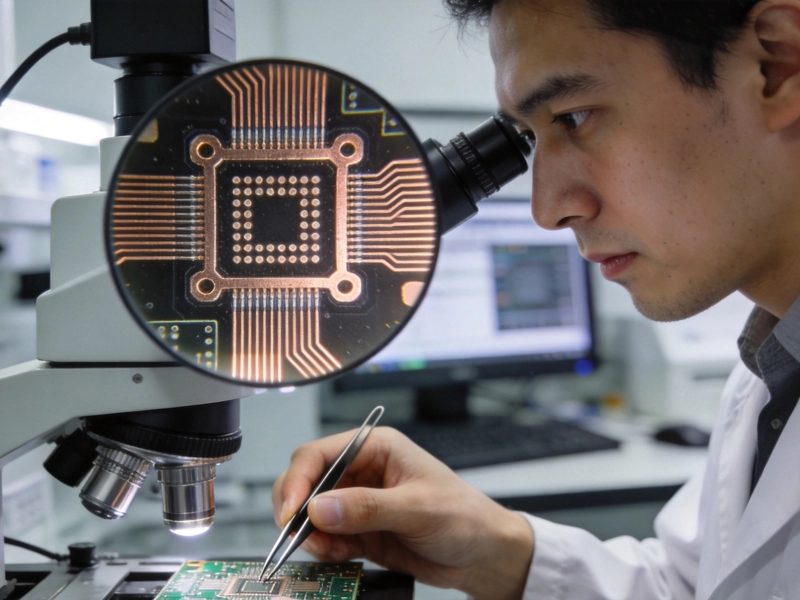
The Role of IPC Standards in HDI PCB Quality AssuranceSeptember/08/2026
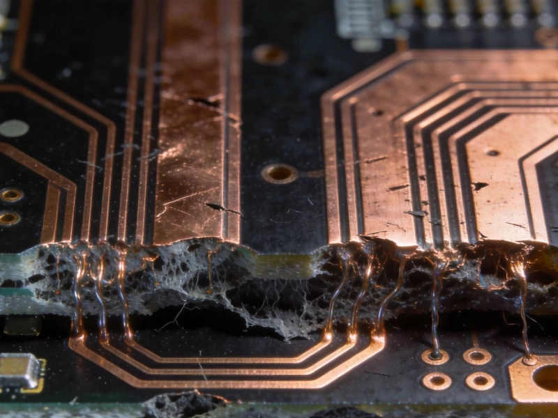
Conductive Anodic Filament (CAF) Resistance in High-Density BoardsJuly/31/2026
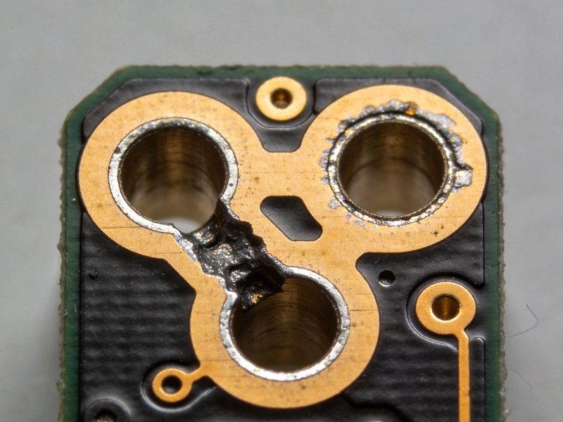
The Impact of Plating Voids on HDI Interconnect ReliabilityJuly/10/2026
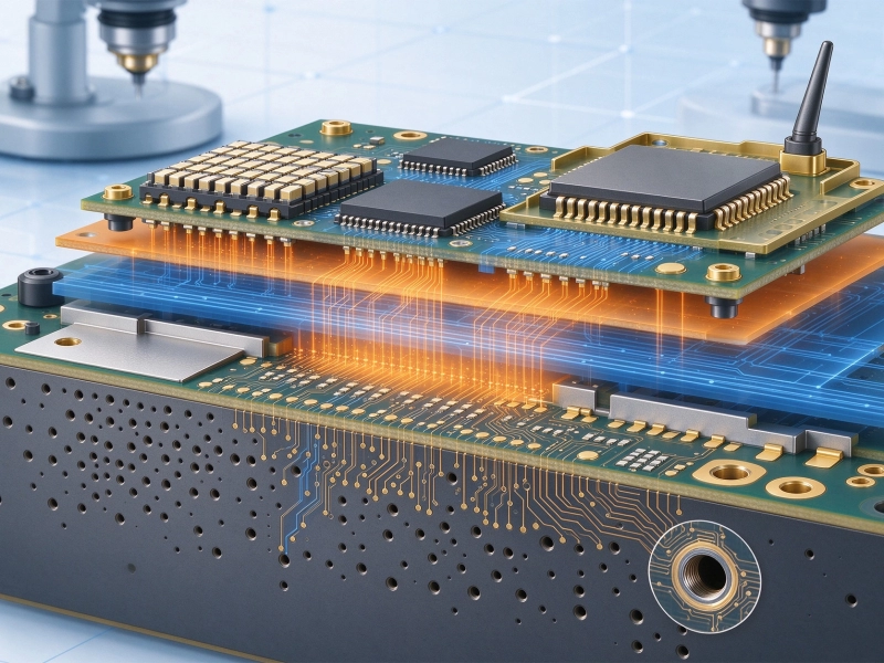
The Impact of HDI on LiDAR and Radar Sensor PerformanceOctober/15/2026
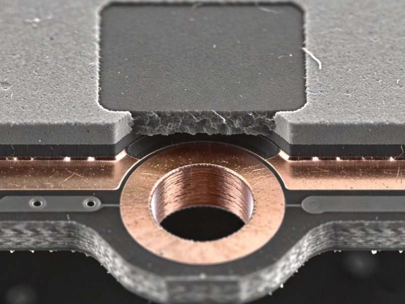
Reliability Challenges of Via-in-Pad Plating Filled (VIPPO) TechnologySeptember/30/2026
Designing HDI Boards to Withstand Extreme Aerospace EnvironmentsJuly/22/2026
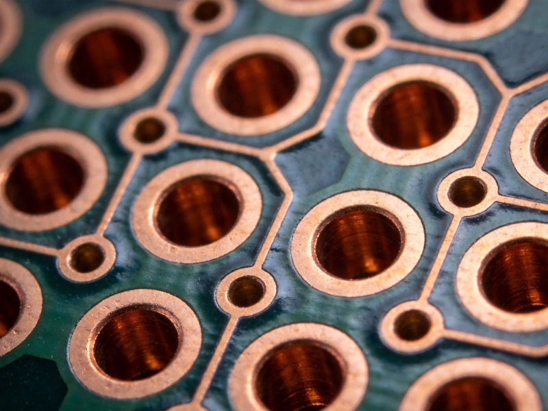
The Importance of Electrical Testing for Microvia ReliabilityJuly/09/2026
Understanding the Core Differences Between HDI and Traditional PCBsJuly/02/2026