Open Nav

Ball Grid Array packaging has become the default choice for modern semiconductor devices, from microprocessors and FPGAs to memory chips and wireless modules. The technology delivers unmatched pin density—today's high-pin-count devices exceed 2,000 connections in packages smaller than a thumbnail. But this density creates routing challenges that push PCB layout engineering to its limits. Get the fanout wrong, and Signal Integrity collapses. Route traces incorrectly, and electromagnetic interference ruins your design. Neglect manufacturing constraints, and your boards won't fab reliably at any price.
This article covers the engineering discipline behind successful BGA fanout and routing in HDI layouts—the practices that separate designs that work from designs that fail mysteriously in the field or during EMC testing.
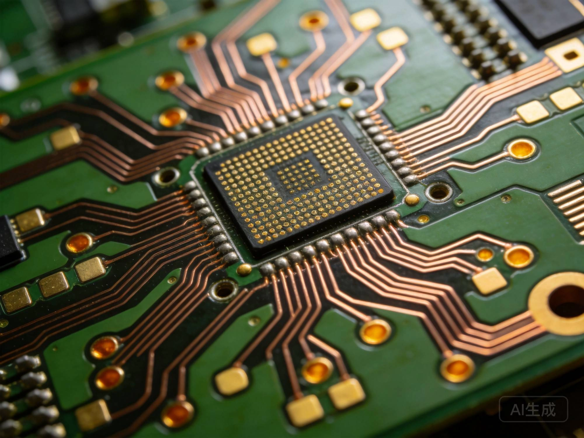
Before diving into specific practices, understanding why BGA fanout presents such difficulty helps frame the engineering decisions that follow.
A BGA component connects to the PCB through an array of solder balls arranged in a grid pattern. The pitch—the center-to-center spacing between adjacent balls—determines how many signals can route through a given area. Standard pitch measures include 1.0mm, 0.8mm, 0.65mm, 0.5mm, 0.4mm, and below. As pitch decreases, routing channels between balls become narrower, and the complexity of escaping all connections from the densely-packed array multiplies rapidly.
Consider a hypothetical 12x12 BGA at 0.5mm pitch. That's 144 connections competing for routing space, and only the outer rows can escape directly outward. Inner rows must route through channels created by the outer rows, requiring vias and layer changes that introduce impedance discontinuities and add manufacturing complexity.
Hdi Technology addresses this challenge by enabling Microvia structures—smaller, more precise vias that can be placed inside the BGA footprint itself. A properly designed HDI stack-up with Sequential Lamination can route signals from the center of a dense BGA to inner layers where routing channels are more abundant, dramatically improving routing efficiency compared to traditional through-hole approaches.
Effective BGA fanout begins by recognizing that different regions of a BGA footprint require different routing strategies. Designers who treat the entire BGA area uniformly miss optimization opportunities and create unnecessary manufacturing challenges.
Escape Zone: The outermost ring of pads requires direct fanout traces that route signals straight out from the component. These traces should follow consistent width rules (matched to the impedance requirements) and maintain consistent spacing from adjacent traces. The escape zone is where manufacturing capability directly constrains design—the minimum trace width and spacing your fabricator can reliably achieve sets the outer boundary of what's possible here.
Intermediate Zone: Interior rows of pins cannot escape directly outward. Signals from these positions must route through channels created by outer row escape routes, or transition through Microvias to inner layers. This zone benefits most from HDI Microvia capabilities, as Microvia Placement allows efficient signal extraction from otherwise inaccessible locations.
Core Zone: The innermost pins of high-pin-count BGAs often have no viable routing through standard microvia strategies. These pins may require advanced techniques like Via-in-pad, blind Buried Via structures, or even multi-level microvia stacking to extract all signals. Some designs simply cannot route all pins at certain pitch levels—the physics and manufacturing constraints are absolute.
Understanding these zones helps designers make intelligent pitch selections during component selection. Choosing a component with marginally larger pitch might eliminate the routing impossibility that would otherwise require expensive advanced HDI processes.
Microvias are the enabling technology that makes dense BGA routing practical in HDI designs. Choosing the right microvia strategy—and implementing it correctly—separates successful layouts from ones that are theoretically routeable but practically unfabricable.
Single-Step vs. Stacked Microvias
Single-step blind microvias connect one layer to an adjacent layer. A via from layer 1 to layer 2, for example, connects top-side components to the first inner layer. These vias are relatively straightforward to fabricate and offer good reliability when properly designed. For BGA fanout, single-step microvias from the top layer to the first inner routing layer handle the majority of escape routing requirements.
Stacked Microvias—directly on top of each other through Sequential Lamination—create vertical interconnection chains that penetrate multiple layers. A stacked via from layer 1 to layer 3 passes through layer 2 en route. This approach provides more routing flexibility but requires careful reliability qualification. Thermal cycling stresses concentrate at the interface between stacked elements, and void-free plating becomes critical to ensure long-term connection integrity.
Via-in-pad Considerations
Via-in-pad (VIP) technology places vias directly in component pads, eliminating the capture pad Annular Ring requirement and recovering significant routing density. For BGA fanout, VIP allows microvias to occupy space that would otherwise be unavailable for routing.
VIP implementations require plug-and-plate processes to create flat pad surfaces for component mounting. The plating process fills the via barrel, then the surface is ground or etched back to expose copper for solder joint formation. Without proper processing, voids in the plating or凹陷 (depressions) at the via center can create solder joint reliability problems.
Design rules for VIP should specify via diameter, plating thickness requirements, and surface flatness tolerances. Your fabricator's VIP capability data sheet provides these specifications—don't design VIP structures without knowing what the manufacturer can actually produce.
BGA fanout routing must maintain controlled impedance for high-speed signals. This requirement interacts with routing density in ways that create engineering tradeoffs.
Standard trace widths for impedance-controlled routing in Hdi Boards typically range from 3 mils (0.075mm) to 5 mils (0.127mm) for 50-ohm single-ended signals. These narrow traces squeeze between BGA pads and microvia capture pads, competing for space in already-dense routing channels.
Several routing strategies address this challenge:
Reference Plane Awareness: Traces routed above solid reference planes (ground or power) maintain predictable impedance more reliably than traces routed over split planes or irregular reference geometries. During BGA fanout, routing assignments should account for which traces need ground reference proximity and route those signals through regions where continuous reference planes exist.
Differential Pair Routing: For differential signals, maintaining consistent coupling between pairs matters as much as individual trace impedance. Design rule checking should verify pair spacing alongside trace width and impedance targets. Route differential pairs through BGA fanout zones first—they have the tightest constraints—and route single-ended signals through remaining channels.
Trace Length Matching: High-speed signals with tight timing budgets require length matching to within tight tolerances. BGA fanout inherently adds length variation as signals route through different paths to escape the component footprint. Budget appropriate length-matching structures in your routing plan, typically serpentine patterns in less-constrained routing regions outside the BGA area.
Effective BGA routing requires thoughtful layer assignment that considers both signal routing needs and manufacturing constraints. The strategy should emerge early in the Stack-up Design phase, not as an afterthought during routing.
A typical HDI stack-up for BGA-heavy designs might look like this:
Layer 1 (Top): Primary component mounting surface. Route escape traces from outermost BGA rows. Place critical components that benefit from minimal loop inductance (power management, high-speed serializers/deserializers).
Layer 2: First inner routing layer. Typically assigned to high-speed signals routing away from the top surface. This layer receives signals from layer 1 microvias and fans them out across the board.
Layers 3-4: Mid-board routing. These layers handle lower-speed signals, power and ground distribution, and less timing-critical interconnects. The layer count depends on overall board complexity and routing density requirements.
Layer N-1 and Layer N (Bottom): Secondary component mounting surface (if needed) and final routing layer. Bottom-side routing often handles escape from BGAs mounted on the bottom side, power/ground reference for bottom-mounted components, and lower-density signal routing.
Power and ground plane assignments typically occupy complete layers rather than sharing layers with signal routing. The plane copper area provides low-impedance distribution and reliable reference plane geometry for controlled-impedance signals. In BGA-intensive designs, allocating dedicated planes for each major power rail simplifies routing congestion in signal layers.
Theoretical routeability means nothing if the design violates manufacturing constraints. DFM (Design for Manufacturability) rules must govern BGA fanout from the earliest layout stages.
Trace Width and Spacing: HDI fabricators achieve 3/3 mil (0.075mm) line/space reliably, with some advanced shops hitting 2/2 mil. Standard rigid PCB shops may struggle below 4/4 mil. Know your fabricator's actual capability—not their marketing claims—and design to that threshold. Relying on 2 mil design rules from a shop that actually achieves 4 mil capability guarantees respin delays.
Microvia Diameter and Capture Pad: Microvia diameters typically range from 4 mils to 8 mils (0.1mm to 0.2mm). Capture pad diameters must accommodate the microvia plus registration tolerance. A common rule: capture pad diameter equals microvia diameter plus 8 mils minimum for standard processes, or microvia diameter plus 5 mils for tight-tolerance advanced processes. Insufficient capture pad margin causes registration errors that create opens.
Annular Ring Requirements: Even with capture pad design rules, microvia lands must maintain minimum annular ring—the copper ring visible around the via barrel on the connection layer. IPC standards specify minimum annular ring requirements (typically 2 mil minimum), but your fabricator's internal capabilities may be tighter. Design to your fabricator's specifications, not generic industry standards.
Dielectric Thickness: HDI microvia aspect ratios (depth to diameter) must stay within fabricator capabilities—typically 0.8:1 to 1:1 for reliable production. Layer thicknesses that produce aspect ratios exceeding this range cause incomplete ablation, barrel voids, or plating failures. Your Stack-up Design must account for the dielectric thicknesses that support reliable microvia formation.
BGA components—especially processors, FPGAs, and high-performance ASICs—draw significant current that must reach the package through the PCB. Power delivery network (PDN) design for BGA components deserves as much attention as signal routing, yet often receives less.
Decoupling Capacitor Placement: High-speed current transients from BGA switching create voltage droop at the package if decoupling is too far away. Place capacitors as close as physically possible to BGA power balls—ideally within the fanout area itself. The loop inductance from capacitor to BGA ball directly affects high-frequency impedance, so proximity matters more than almost any other factor.
Via Count Requirements: Power and ground balls at each BGA corner and along edges need dedicated vias carrying current from plane layers to the component. These vias must handle current density without excessive resistance or heating. Calculate current per ball based on total power consumption, number of power balls, and acceptable current density (typically below 20-30 mA per via for reliable long-term operation).
Plane Connectivity: Ensure continuous low-impedance paths from decoupling capacitors through via networks to power and ground planes. Any constriction in current flow—narrow neck regions, insufficient via count, reference plane slots—creates impedance that degrades PDN performance. Use current density verification tools during design review to identify potential problems.
High-speed signals routing through BGA fanout areas face several integrity threats that require proactive mitigation during layout.
Impedance Discontinuity: Every via, pad entry, and geometry change creates impedance discontinuity. The fanout zone concentrates these discontinuities—multiple vias in close proximity, varying trace widths, reference plane interruptions. While eliminating discontinuities is impossible, minimizing their impact requires keeping high-speed routing away from the most discontinuity-dense fanout regions when possible.
Via Stub Effects: Non-functional via stubs—portions of via barrel extending beyond the signal routing layer—create resonant cavities that absorb signal energy at specific frequencies. For high-speed serial links above 10Gbps, even short stubs matter. Back-drilling through-hole vias removes non-functional barrel, but microvia structures require different approaches—designing microvia depth carefully or using blind microvia structures that don't extend beyond the signal path.
Crosstalk in Dense Routing: BGA fanout creates parallel trace sections where signals run adjacent for short distances before separating to their destinations. Coupling between traces causes crosstalk that degrades signal-to-noise ratio. Maintain consistent trace spacing (and ground trace spacing guidelines for differential pairs) through fanout regions. Route aggressor and victim pairs in different layers when fanout geometry forces long parallel sections.
Differential interfaces—USB, PCIe, HDMI, SerDes links—appear in virtually every modern BGA component. Routing these pairs through BGA fanout zones requires special attention beyond standard Impedance Control.
Pair Skew Control: Differential signals require tight matching between pair members—typically 5-10 mils maximum intra-pair skew for 10Gbps+ interfaces. Bga Escape Routing inevitably routes pair members through different path lengths as they route around other signals. Budget length-matching structures outside the fanout zone to compensate for escape routing imbalance.
Pair Spacing Consistency: Maintain consistent coupling (spacing between pair members) throughout the routing. Variations in spacing change Differential Impedance, creating mode conversion that turns differential signals into unwanted common-mode energy. Design rules should enforce minimum spacing as well as maximum—don't let auto-routing algorithms spread pairs apart in fanout regions.
Reference Plane Continuity: Differential pairs should route over continuous reference planes to maintain predictable common-mode return paths. Routing over split planes, near board edges, or over gaps in reference geometry creates impedance variation and common-mode excitation. Assign differential pairs to routing layers with solid plane reference, even if it means routing less-critical single-ended signals in less-optimal regions.
BGA components generate significant heat that must dissipate through the PCB. Thermal Management intersects with BGA routing in ways that affect both electrical performance and long-term reliability.
Thermal Via Arrays: Many BGA packages include thermal balls (center array) designed specifically for heat transfer to the PCB. Route Thermal Vias from these balls to ground planes or dedicated thermal dissipation layers. Via diameter and count affect thermal resistance—more vias with larger diameters lower thermal resistance more effectively.
Power Plane Thermal Contribution: Power planes distribute heat as well as current. Allocating adequate copper area for power planes in BGA regions helps spread heat from the component. However, thermal spreading competes with routing channels—balance thermal needs against routing density requirements.
Component Placement Interactions: Components placed near BGA devices affect thermal behavior. Hot components placed near temperature-sensitive circuits create thermal coupling that may degrade performance or reliability. Consider thermal interactions during overall board layout, not just within the BGA fanout zone.
Thorough verification before manufacturing catches errors that would otherwise cause expensive respins or field failures. BGA-intensive designs warrant particularly careful review.
Design Rule Checking: Automated DRC should verify all fanout-related constraints: minimum trace width and spacing, minimum annular ring, via capture pad coverage, Impedance Tolerance, differential pair matching, and layer assignment correctness. Configure DRC to catch fanout-specific violations, not just generic electrical rules.
Signal Integrity Simulation: For high-speed interfaces, simulate channel performance through the BGA fanout region. Extract S-parameters or run time-domain simulation to verify that fanout discontinuities don't degrade signals beyond acceptable limits. This verification is especially critical for 10Gbps+ serial links where fanout-related losses and reflection compound.
Fabricator Communication:
Before finalizing your design, share the layout with your fabricator for DFM review. Most reputable HDI manufacturers offer design-for-manufacturability feedback that identifies potential problems before they become production failures. This collaboration often reveals design rule adjustments or layout modifications that improve yields without affecting electrical performance.
Understanding common errors helps designers avoid them. Several mistakes appear repeatedly in BGA layouts that don't receive adequate review.
Underestimating Routing Complexity: Designers who plan routing based on simple channel counting miss the reality of practical constraints. Every fanout channel must accommodate trace width, spacing, reference requirements, and manufacturing tolerances. Rule-of-thumb channel estimates should be validated against actual design rules before committing to component selection.
Ignoring Layer-to-Layer Registration: Microvia structures stack across layers, and each layer transition adds registration tolerance. Stacked microvias accumulate this tolerance across multiple layers, potentially causing registration failures that simple single-layer analysis misses.
Neglecting Return Path Integrity: Signal return currents flow through reference planes, and any break in the reference plane under a high-speed trace forces return currents to travel far from the signal path. This increases loop inductance and creates EMI problems. Verify reference plane continuity for all high-speed signals, including their paths through fanout regions.
Forgetting Manufacturing Test Access: Dense BGA routing sometimes consumes all available routing channels, leaving no space for test points or probing access. Building in adequate test access—particularly for high-speed signals that require in-circuit characterization—prevents manufacturing difficulties that surface only after boards return from assembly.
The relationship between PCB designer and fabricator significantly affects BGA routing success. Early collaboration yields better outcomes than adversarial relationships where designers throw designs over the wall for manufacturing to either succeed or fail.
Share your design constraints and priorities. Which signals are most critical? What timing margins exist? What are the thermal requirements? This context helps fabricators recommend design modifications that improve manufacturability without compromising your design goals.
Ask about capability limits. What minimum trace/space can they actually achieve on your production volume? What microvia aspect ratios work reliably? What capture pad designs yield best results? Fabricators with extensive HDI experience have process data that improves design outcomes.
Request cross-section data from previous similar designs. This verification demonstrates actual process capability in terms of achievable geometries—not just theoretical specifications.
For the most demanding BGA packages—those below 0.4mm pitch or with complex 3D stacking requirements—standard HDI approaches may prove insufficient. Several advanced techniques address these extreme cases.
Any-layer Hdi (ALH): Full any-layer interconnect allows microvias to connect any two layers in the stack, providing maximum routing flexibility. ALH processes accept significant cost premiums but enable routing densities impossible with simpler sequential buildup strategies.
Substrate-Like PCB (SLP): SLP technology borrows semiconductor substrate manufacturing approaches for PCB-scale integration. Feature sizes shrink dramatically—lines and spaces below 30 microns—enabling routing densities approaching chip-scale packages.
Embedded Active Components: Some designs embed bare die directly within the PCB stack, eliminating BGA fanout entirely for those components. This approach trades manufacturing complexity for routing simplification.
Mastering BGA fanout and routing in HDI layouts requires integrating electrical design, manufacturing knowledge, and signal integrity discipline into every layout decision. The best practices aren't arbitrary rules—they emerge from understanding the physics of signal transmission, the capabilities of manufacturing processes, and the reliability requirements of end applications. Designers who build this knowledge develop layouts that work reliably the first time, manufacturable at reasonable cost, and scalable across production volumes. Those who treat BGA routing as a puzzle to solve with routing channels alone invite the respins, failures, and schedule delays that plague less-careful approaches.
Non-Destructive Testing Techniques for Multilayer HDI PCBsSeptember/29/2026

A Step-by-Step Walkthrough of the HDI PCB Manufacturing ProcessMay/28/2026
The Importance of Electrical Testing for Microvia ReliabilityJuly/09/2026

Advanced Testing Methods for High-Density Interconnect PCBsMay/28/2026

Overcoming the Challenges of Testing Fine-Pitch BGA on HDISeptember/04/2026

Mastering Stack-up Design for Optimal HDI PerformanceJune/08/2026
Designing for Manufacturing (DFM): Avoiding Common HDI PitfallsSeptember/02/2026

Flying Probe vs. Fixture Testing: Which is Best for HDI PCBs?June/11/2026