
High-density Interconnect designs compress more routing into less space, which makes Impedance Control both more critical and more difficult. The physics of impedance does not change — controlled impedance still depends on trace geometry, dielectric properties, and reference plane distance. What changes in HDI is how much margin you have to get it right. Smaller traces, thinner dielectrics, and via transitions all tighten the tolerance window. A mistake that would be absorbed in a conventional design becomes a Signal Integrity problem in HDI.
This article explains how to implement Impedance Control effectively in HDI designs. We will cover stack-up planning, trace geometry constraints, Microvia effects, via stub management, and the manufacturing tolerances that determine whether your impedance targets are achievable in production.
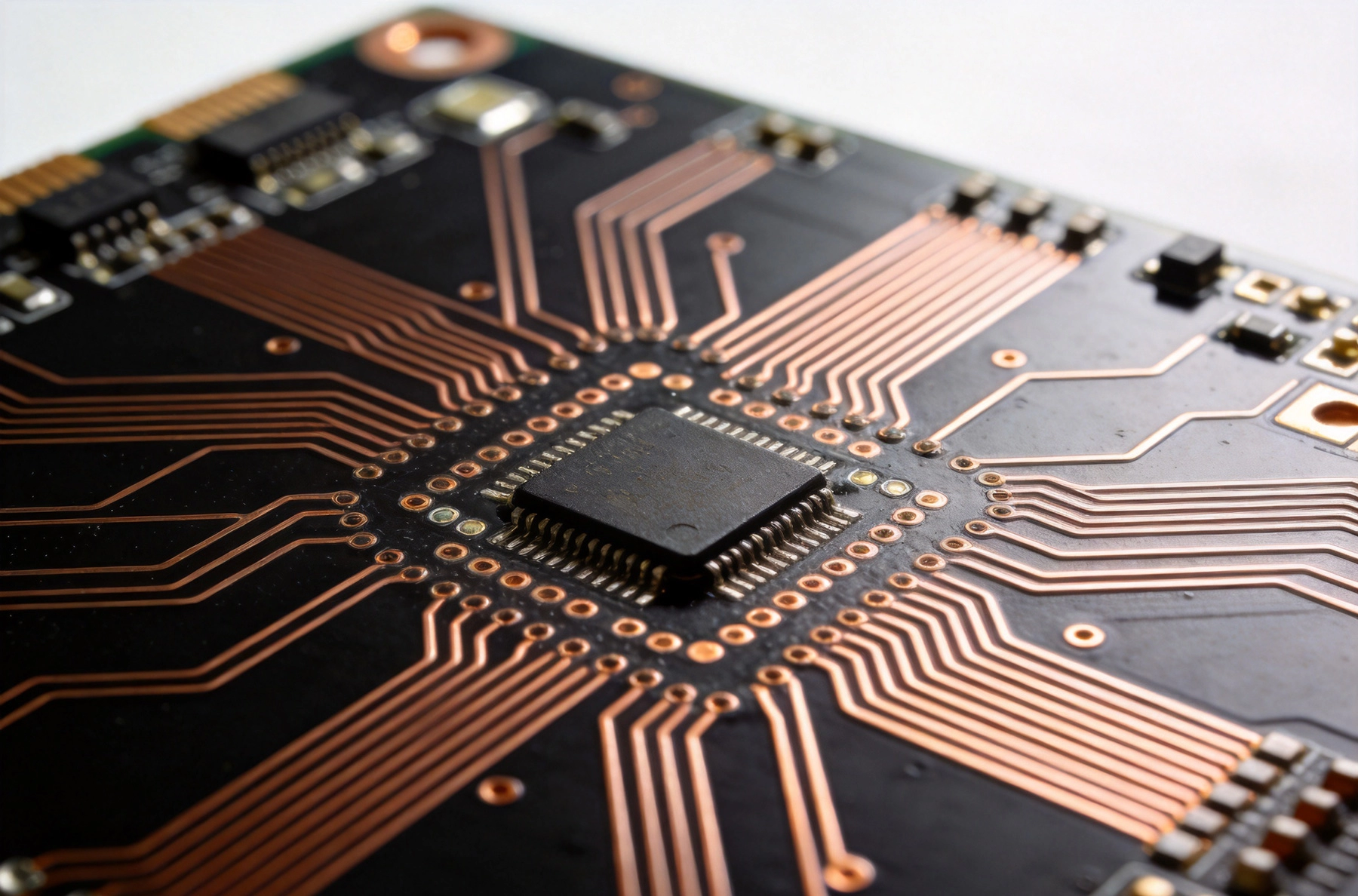
HDI designs use finer features than conventional PCBs. Trace widths of 75 microns or less are common. Dielectric thicknesses between layers can be 50 microns or thinner. Microvias connect layers without the barrel length of through-hole vias. These characteristics are what enable HDI density, but they also change the impedance equation.
Thinner dielectrics reduce the distance between signal traces and reference planes, which increases capacitance per unit length. To maintain the same impedance, trace width must decrease. Narrower traces are harder to manufacture with consistent width. The width tolerance as a percentage of nominal becomes larger, which translates directly to impedance variation.
Microvias introduce discontinuities in the signal path. A via transition changes the effective dielectric environment around the trace. The via pad adds capacitance. The via barrel adds inductance. These discontinuities cause impedance perturbations that degrade Signal Integrity at high speeds. Managing via effects is essential for effective HDI impedance control.
Impedance control starts with stack-up planning. The layer order, dielectric thickness, and material selection determine what trace geometries are achievable.
For controlled impedance traces, the ratio of trace width to dielectric height is the primary design parameter. Thicker dielectrics allow wider traces for the same impedance, which improves manufacturing yield. Thinner dielectrics enable tighter routing density but require narrower traces that are harder to control.
In HDI stack-ups, the thin dielectric layers are often defined by the Microvia build-up process. A typical microvia layer might use prepreg or resin-filled dielectric at 40 to 60 microns thickness. Controlled impedance traces on these layers will have narrow widths. Specify the dielectric thickness tolerance explicitly — standard prepreg tolerance is approximately plus or minus 10 percent, which directly affects Impedance Tolerance.
The dielectric constant of the substrate material affects impedance. Standard FR-4 has a Dk around 4.4 to 4.8 with tolerance around plus or minus 10 percent. For tight Impedance Tolerance, this material variation is too large. High-speed materials with tighter Dk tolerance — plus or minus 2 percent or better — reduce material-driven impedance variation.
Material Dk also varies with frequency. FR-4 Dk decreases at higher frequencies, which changes impedance across the signal bandwidth. For high-speed digital designs above 5 gigabits per second, choose materials with flat Dk versus frequency characteristics.
Symmetrical stack-ups — where the layer sequence from top to bottom mirrors from bottom to top — reduce warpage and improve registration control during lamination. For impedance-controlled designs, symmetrical construction helps maintain consistent dielectric thickness across the panel. Asymmetric stack-ups can work but require more careful process control.
Once the stack-up is defined, trace geometry determines impedance. For effective impedance control, follow these routing principles.
Use field solver software to calculate trace width for your target impedance given the stack-up parameters. Do not rely on simple approximations — HDI geometries are often outside the range where empirical formulas are accurate. The field solver should account for trace thickness, solder mask coverage, and copper roughness effects.
For differential pairs, calculate trace width and spacing together. Differential Impedance depends on both parameters. The coupling between traces affects impedance; closer spacing reduces Differential Impedance for the same trace width.
Manufacturing tolerance on trace width directly impacts impedance tolerance. For a 75 micron trace with a plus or minus 15 micron width tolerance, the width can vary by 20 percent. For 50 ohm lines, this translates to impedance variation of approximately plus or minus 5 to 7 percent from width alone.
For tighter impedance tolerance, specify trace width tolerance to the fabricator. Tighter width tolerance requires tighter process control and may increase cost. Know what tolerance is achievable on your fabricator's process before finalizing impedance targets.
Impedance depends on distance to the reference plane. If the reference plane has voids or splits near the controlled impedance trace, impedance changes at those locations. Route controlled impedance traces over continuous reference plane areas. Avoid routing over plane splits or voids unless the design explicitly requires it.
For stripline traces — embedded between two reference planes — the distance to each plane matters. Uneven spacing creates asymmetrical impedance. Design stack-ups so controlled impedance striplines are centered between reference planes.
Microvias are essential to HDI routing density, but they introduce impedance discontinuities that require management.
When a signal transitions between layers through a microvia, the impedance changes. The via pad adds capacitance. The via barrel and capture pad add inductance. The net effect is an impedance discontinuity that causes reflections at high speeds.
To minimize discontinuity, use the smallest practical via pad diameter. Larger pads add more capacitance. Use Via-in-pad structures where the via is placed directly under the component pad rather than using a separate via pad with trace routing.
For through-hole vias, the unused portion of the via barrel below the target layer creates a stub that acts as a resonant structure. At frequencies where the stub length is a quarter wavelength, the stub causes significant signal degradation. For high-speed signals, eliminate via stubs by using blind or Buried Vias that only extend through the necessary layers, or use back-drilling to remove the stub.
Microvias inherently avoid stub problems because they only extend one layer. This is an advantage for high-speed HDI designs — use microvias for high-speed signal transitions rather than through-hole vias where stubs would be an issue.
For differential pairs, both signals should transition layers through matched via structures. Matching means the via geometry, pad size, and antipad clearance are the same for both vias. The via spacing should match the differential pair spacing. Mismatched vias convert common-mode noise to differential noise and degrade signal integrity.
Controlled impedance designs require verification through testing. Plan for impedance testing early in the project.
Impedance is measured on test coupons that run alongside the production panel. The coupon must use the same stack-up construction, trace geometry, and materials as the production traces. A coupon that does not match the production design will give misleading impedance data.
Include single-ended and differential test structures as needed. Provide access for time-domain reflectometry probes. The coupon traces should be long enough for accurate measurement — typically several centimeters depending on the Tdr system.
Specify impedance tolerance explicitly. Standard tolerance is plus or minus 10 percent. For high-speed designs, specify tighter tolerance such as plus or minus 7 percent or plus or minus 5 percent. Tighter tolerance requires tighter material Dk control, tighter trace width tolerance, and tighter dielectric thickness control.
Confirm with your fabricator that the specified tolerance is achievable on their process. Request impedance test data on the first article to verify that the process meets the specification.
Effective impedance control requires understanding what tolerances are achievable and designing margin accordingly.
Dielectric thickness tolerance varies by material and construction. Standard prepreg tolerance is approximately plus or minus 10 percent. Controlled depth builds may achieve plus or minus 5 percent. For tight impedance tolerance, specify thickness tolerance and verify capability with your fabricator.
Trace width tolerance depends on the fabrication process. Standard tolerance for HDI trace widths is approximately plus or minus 20 percent of the nominal width. Tighter tolerance of plus or minus 10 percent is achievable with controlled processes. The relationship between width tolerance and impedance tolerance is approximately linear for typical geometries.
Copper thickness affects impedance. Standard Copper Plating tolerance is approximately plus or minus 10 percent for typical copper weights. For thin copper layers used in HDI, plating uniformity becomes more critical. Specify copper thickness tolerance for controlled impedance layers.
Material Dk tolerance contributes to impedance variation. Standard FR-4 Dk tolerance is plus or minus 10 percent. High-speed materials offer plus or minus 2 percent or better Dk tolerance. Select material based on your impedance margin requirements.
Experience from HDI design reviews shows recurring patterns that undermine impedance control:
Routing over reference plane splits. Controlled impedance traces that cross plane voids or splits experience impedance discontinuities. Route over continuous copper. If splits are unavoidable, understand the impedance impact and account for it in signal integrity analysis.
Inadequate test coupon design. A coupon that uses different trace width, spacing, or layer construction than the production traces provides misleading data. Design coupons that exactly match production geometry.
Ignoring via effects. Treating vias as transparent interconnects ignores their impedance impact. Model via transitions in signal integrity simulation. Use appropriate via geometries for high-speed signals.
Specifying tighter tolerance than the process can deliver. A plus or minus 5 percent impedance specification is meaningless if the fabricator's process cannot achieve it. Confirm process capability before committing to tight tolerances.
Effective impedance control in HDI requires collaboration with your fabricator. Engage early in the design process.
Share your stack-up requirements, impedance targets, and tolerance needs. Ask the fabricator to confirm capability. Request their stack-up recommendations for your target impedance — they may suggest adjustments that improve manufacturability.
For first articles, request impedance test data from the production coupon. Review the data against your specification. If impedance is outside tolerance, work with the fabricator to identify the root cause — trace width, dielectric thickness, or material Dk — and adjust the process accordingly.
The required trace width depends on dielectric thickness, material Dk, and trace thickness. For a typical HDI build with 50 micrometer dielectric and Dk of 4.2, 50 ohm single-ended impedance might require a trace width of approximately 60 to 80 micrometers. Use a field solver to calculate exact dimensions for your specific stack-up.
Smaller via diameter reduces the impedance discontinuity at the via transition. The via pad capacitance scales with pad area. Smaller pads — enabled by smaller via diameter — reduce capacitance and minimize impedance perturbation. For high-speed signals, use the smallest via geometry that meets your fabricator's capability.
Yes, for applications with moderate impedance tolerance requirements and data rates below 5 gigabits per second. Standard FR-4 Dk tolerance of plus or minus 10 percent limits achievable impedance tolerance. For tighter tolerance or higher data rates, use high-speed materials with controlled Dk and loss characteristics.
Differential impedance depends on trace width, trace spacing, and distance to reference planes. Control all three parameters. Use tightly coupled differential pairs with spacing approximately equal to trace width. Maintain consistent spacing throughout the route. Match the trace widths of both conductors. Model the differential pair in a field solver to verify impedance.
Plus or minus 10 percent is achievable with standard processes and materials. Plus or minus 7 percent requires tighter process control and materials with better Dk tolerance. Plus or minus 5 percent is achievable with high-speed materials and carefully controlled processes but adds cost. Discuss your tolerance needs with your fabricator to understand what is achievable and at what cost.
Non-Destructive Testing Techniques for Multilayer HDI PCBsSeptember/29/2026
Designing HDI Backplanes for High-Performance Networking EquipmentOctober/16/2026
Best Practices for BGA Fanout and Routing in HDI LayoutsJuly/07/2026
The Importance of Electrical Testing for Microvia ReliabilityJuly/09/2026

Mastering Stack-up Design for Optimal HDI PerformanceJune/08/2026
How X-Ray Inspection (AXI) Detects Hidden Defects in HDI BoardsJuly/30/2026
The Art of Microvia Placement: Staggered vs. Stacked ViasSeptember/24/2026

Flying Probe vs. Fixture Testing: Which is Best for HDI PCBs?June/11/2026