
Open any smartphone, peel back the EMI shield, and look at the main PCB. What you see is a board roughly the size of a credit card carrying an application processor with 2,000+ solder balls on 0.35 mm pitch, 8–16 GB of LPDDR memory in a package-on-package stack, a mmWave antenna module, hundreds of 0201 and 01005 passive components, and dozens of high-speed differential pairs routing between them—all on 10 or more layers with feature sizes that were considered advanced semiconductor geometry a generation ago. That board is an HDI (High-density Interconnect) PCB, and without Hdi Technology, the device you are holding would be the size of a brick.
HDI is not a single innovation but a suite of manufacturing capabilities—Microvias, fine lines, build-up layers, Via-in-pad, and any-layer interconnect—that together enable the component density, routing density, and signal-integrity performance that modern electronics demand. This article examines how each of these capabilities works, why they matter, and how they are transforming product design across industries.
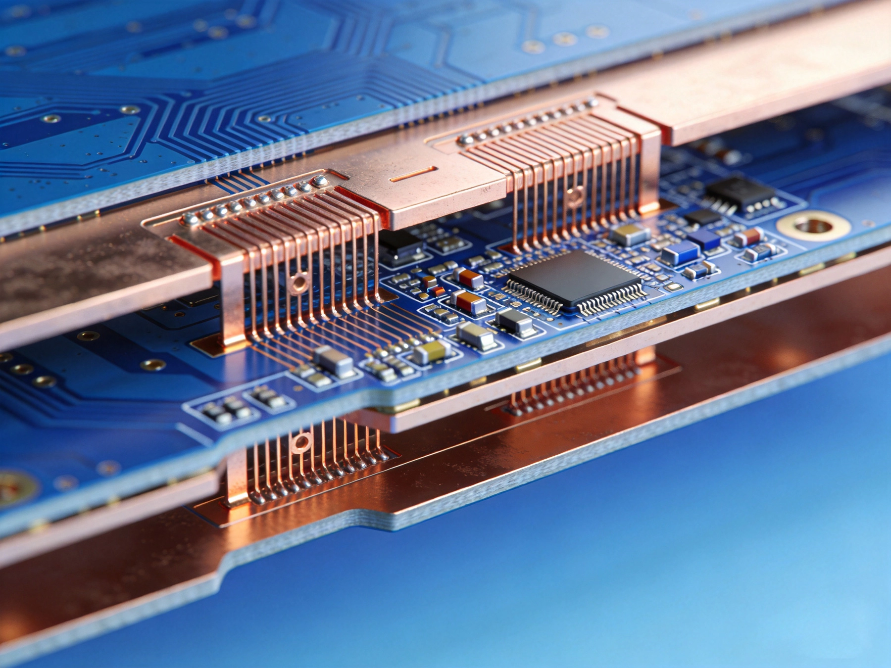
A conventional PCB (sometimes called a "through-hole multilayer" or THML board) uses plated through-holes (PTHs) to connect layers. A 1.0 mm diameter PTH on a 1.6 mm board consumes a via pad on every layer plus an Annular Ring—typically 2.0–2.5 mm total diameter on every layer, whether that layer needs the connection or not. On a dense board, PTHs consume 40–60 % of available routing area, creating a "Swiss cheese" effect that limits how many traces can route between vias.
Hdi Boards replace large PTHs with Microvias—small-diameter, short-depth vias that connect only adjacent layers. A typical Microvia is 0.1 mm diameter, connecting two adjacent layers over a 0.05–0.1 mm dielectric. Because it is small and local, it consumes minimal routing area on other layers. The result: dramatically higher interconnect density, finer routing channels, and the ability to escape-route from fine-pitch BGAs that would be impossible on a THML board.
The IPC-2226 standard defines Hdi Boards by their feature sizes and via structures:
Unlike through-holes, which are drilled mechanically, microvias are created by Laser Drilling. A UV or CO₂ laser ablates a small hole through the dielectric layer to expose the target pad on the layer below. The hole is then desmeared (removing residual dielectric resin from the copper target) and metallized—typically by electroless copper deposition followed by electrolytic Copper Plating, or by conductive-ink fill followed by planarization.
Laser-drilled microvia capability defines what a fab can produce:
For Via-in-pad construction (where a component pad sits directly over a via), the microvia must be filled with copper or epoxy-copper paste and planarized flat. Unfilled vias under BGA pads would wick solder away from the joint during reflow, creating open or weak connections. Via Filling adds process steps (fill, planarize, cap-plating) but is essential for fine-pitch BGA breakout routing.
For most high-speed applications, stacked microvias are preferred for their lower parasitic inductance (typically 0.2–0.4 nH per via vs. 0.5–0.8 nH for staggered with a short trace). The difference matters at 10+ Gbps, where via parasitics can degrade Signal Integrity.
HDI boards routinely use trace widths and spaces of 3/3 mil (0.075/0.075 mm) or even 2/2 mil (0.050/0.050 mm) in the build-up layers. This compares to 4/4 or 5/5 mil on conventional boards. Fine-line routing is what allows HDI to escape-route from 0.4 mm pitch BGAs with room to spare.
The combination of microvias and fine lines multiplies routing density. On a conventional 4/4 mil board with through-holes, a 0.5 mm pitch BGA typically allows one trace between via pads (sometimes called "1-line channel"). On an HDI board with 3/3 mil lines and microvias, the same BGA allows two or three traces between via pads. This is the difference between a routable and an unroutable design.
HDI boards are built in a fundamentally different sequence from conventional multilayer boards. Instead of laminating all layers at once, HDI uses a sequential build-up process:
Each build-up lamination cycle adds cost and cycle time. A Type I HDI (one build-up per side) adds one lamination cycle. A Type III HDI (two build-ups per side) adds two. An Any-layer Hdi with N layers adds N−2 cycles. This is why HDI is more expensive than THML—but the cost is justified when the alternative is a larger board or a product that cannot meet its size target.
On a conventional board, BGA pads cannot have vias in them—vias are placed in the "dog-bone" area between pads, with a short trace connecting the pad to the via. At 0.5 mm pitch, the dog-bone area is barely large enough for a 0.25 mm via. At 0.4 mm pitch, it is impossible—the via must go in the pad.
Via-in-pad (VIP) places a filled microvia directly in the BGA land pad. The via connects the pad to the target layer without any routing channel on the component side. This:
VIP requires filled-and-capped microvias (as described above) and careful thermal design—the via conducts heat away from the BGA joint, which can affect solder-joint reliability for components with low thermal mass. Simulation and reliability testing are recommended for VIP under 0.4 mm pitch components in thermally demanding applications.
The smartphone is the canonical HDI application. A flagship phone main board is typically a 10–14 layer any-layer HDI with:
Without any-layer HDI, a phone board of equivalent functionality would be 3–5× larger—unacceptable in a market where every millimeter of device thickness is competitive advantage.
True wireless earbuds, smartwatches, and AR glasses push HDI further—into boards under 10 mm × 20 mm with 6–8 layers and 2/2 mil lines. These ultra-small HDI boards often use embedded components (passives buried in inner layers) to further reduce surface area. The via density is extreme: some wearable HDI boards have over 10,000 microvias per square centimeter.
Pacemakers, neurostimulators, and cochlear implants use HDI to maximize functionality within the smallest possible hermetic package. A modern pacemaker PCB is a 6–8 layer HDI board under 30 mm × 20 mm, carrying a system-on-chip, telemetry antenna, sensing channels, and therapy output stages. HDI enables the routing density needed to interconnect these functions in the limited board area, while the thin build-up construction helps meet the package-height constraint of a subcutaneous implant.
Automotive Electronics are not yet at smartphone-level HDI density, but the trend is accelerating. Adas domain controllers—centralized compute platforms that process data from radar, camera, and lidar sensors—are migrating from 6–8 layer THML boards to 10–12 layer Type II/III HDI boards. The driver is the processor: NVIDIA Orin, Qualcomm Ride, and similar SoCs come in 0.4 mm pitch BGAs with 1,500+ balls. Routing these on a THML board requires an unacceptably large board or a processor package with fewer I/O (sacrificing performance). HDI provides the escape routing density in the board area that the vehicle packaging allows.
5G new-radio modules operate at 28 GHz and 39 GHz, requiring antenna-in-package (AiP) or antenna-on-board constructions with precise controlled-impedance routing and tight dielectric thickness control. HDI build-up layers provide the thin, controlled dielectrics (50–100 µm) needed for mmWave microstrip and stripline structures—thicknesses that are difficult to achieve in a conventional core-based stack-up. The microvias connecting the antenna elements to the RF transceiver must have minimal parasitic inductance, favoring stacked microvias in the feed network.
HDI design involves a different set of trade-offs than conventional Pcb Design:
Not every PCB manufacturer can produce HDI boards, and the capability range varies widely. When evaluating an HDI fabricator, assess:
The demand for Miniaturization shows no sign of abating, and Hdi Technology continues to evolve to meet it:
HDI technology is the enabler of modern electronics Miniaturization—not a luxury but a necessity for any product that must pack high functionality into a small space. Microvias, fine lines, build-up laminations, and via-in-pad construction work together to provide interconnect density that conventional through-hole multilayer boards cannot approach. The result is smaller products, higher performance (shorter interconnects mean better signal integrity), and new form factors that were literally impossible before HDI.
The cost premium of HDI over conventional boards is real but often overstated. For many designs, HDI is the only way to route the board in the available area—and the alternative (a larger board, a larger product, or a less capable processor) is far more costly. As component pitches continue to shrink and interconnect counts continue to rise, HDI is not just the best option—it is the only option that scales.
For HDI PCB Fabrication with any-layer microvia capability, fine-line SAP/mSAP processes, and proven reliability data, contact our HDI engineering team to discuss your stack-up and routing requirements.
HDI boards use microvias (laser-drilled, small-diameter vias connecting adjacent layers) and fine trace widths (3 mil or below) instead of the large through-holes and wider traces of conventional boards. This dramatically increases routing density, enabling finer-pitch component breakout and smaller board sizes.
Any-layer HDI (Type IV) connects every layer pair with microvias—there are no through-holes spanning the entire board. This provides the highest interconnect density and is used in the most advanced smartphones and wearable devices.
Microvias have much lower parasitic inductance (0.2–0.4 nH vs. 0.5–1.5 nH for through-holes) because of their smaller diameter and shorter length. Lower inductance means less signal degradation at high frequencies, improving eye-diagram margin at multi-gigabit data rates.
Via-in-pad places a filled microvia directly inside a BGA land pad, eliminating the "dog-bone" trace that connects the pad to a nearby via. It is required for BGA pitches of 0.5 mm and below, where there is no space between pads for a separate via and connecting trace.
Cost depends on the HDI type and layer count. Type I HDI (one build-up per side) typically adds 20–30 % over a comparable THML board. Type III HDI adds 50–80 %. Any-layer HDI can cost 2–3× a conventional board. However, HDI often eliminates the need for a larger board or an interposer, so system-level cost may be lower.
Challenges of Integrating HDI in High-Efficiency Power InvertersJuly/16/2026
HDI Applications in Advanced Battery Management Systems (BMS)June/18/2026
The Role of HDI in Smart Grid and Energy Storage SystemsAugust/06/2026
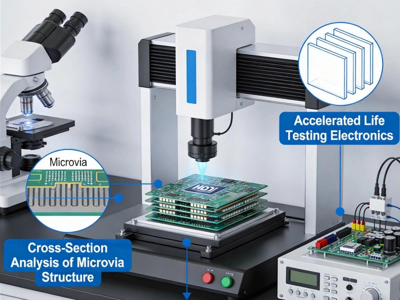
Key Factors Influencing the Long-Term Reliability of HDI PCBsMay/28/2026
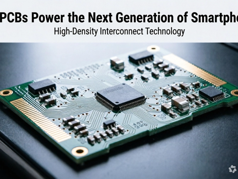
How HDI PCBs Power the Next Generation of SmartphonesJune/17/2026
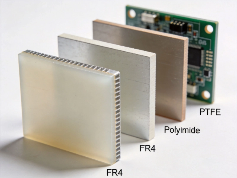
Selecting the Right Dielectric Materials for High-Performance HDI PCBsMay/28/2026
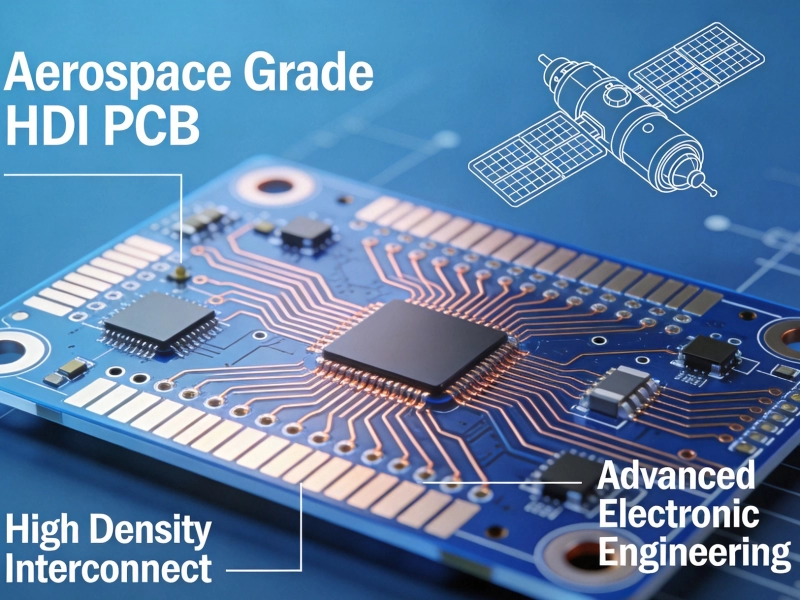
Designing HDI Boards to Withstand Extreme Aerospace EnvironmentsJuly/22/2026
HDI Solutions for High-Performance Gaming Consoles and LaptopsSeptember/10/2026