Open Nav

Autonomous driving and advanced driver-assistance systems (ADAS) rely on a continuous stream of high-fidelity sensor data. LiDAR and radar are the two primary perception technologies enabling vehicles to "see" their surroundings, but their performance is only as good as the printed circuit boards that carry their signals. As sensor resolution, operating frequency, and integration density increase, Traditional Pcb architectures are no longer sufficient. This is where The Impact of HDI on LiDAR and Radar Sensor Performance becomes a defining factor in next-generation Automotive Electronics.
High Density Interconnect (HDI) technology is not merely a space-saving convenience. It is a performance enabler that directly influences Signal Integrity, thermal behavior, mechanical reliability, and ultimately the accuracy of LiDAR and radar systems. In this article, I will examine how HDI structures affect sensor performance, where HDI adds real value, and where its limitations must be managed through material selection and Stack-up Design.
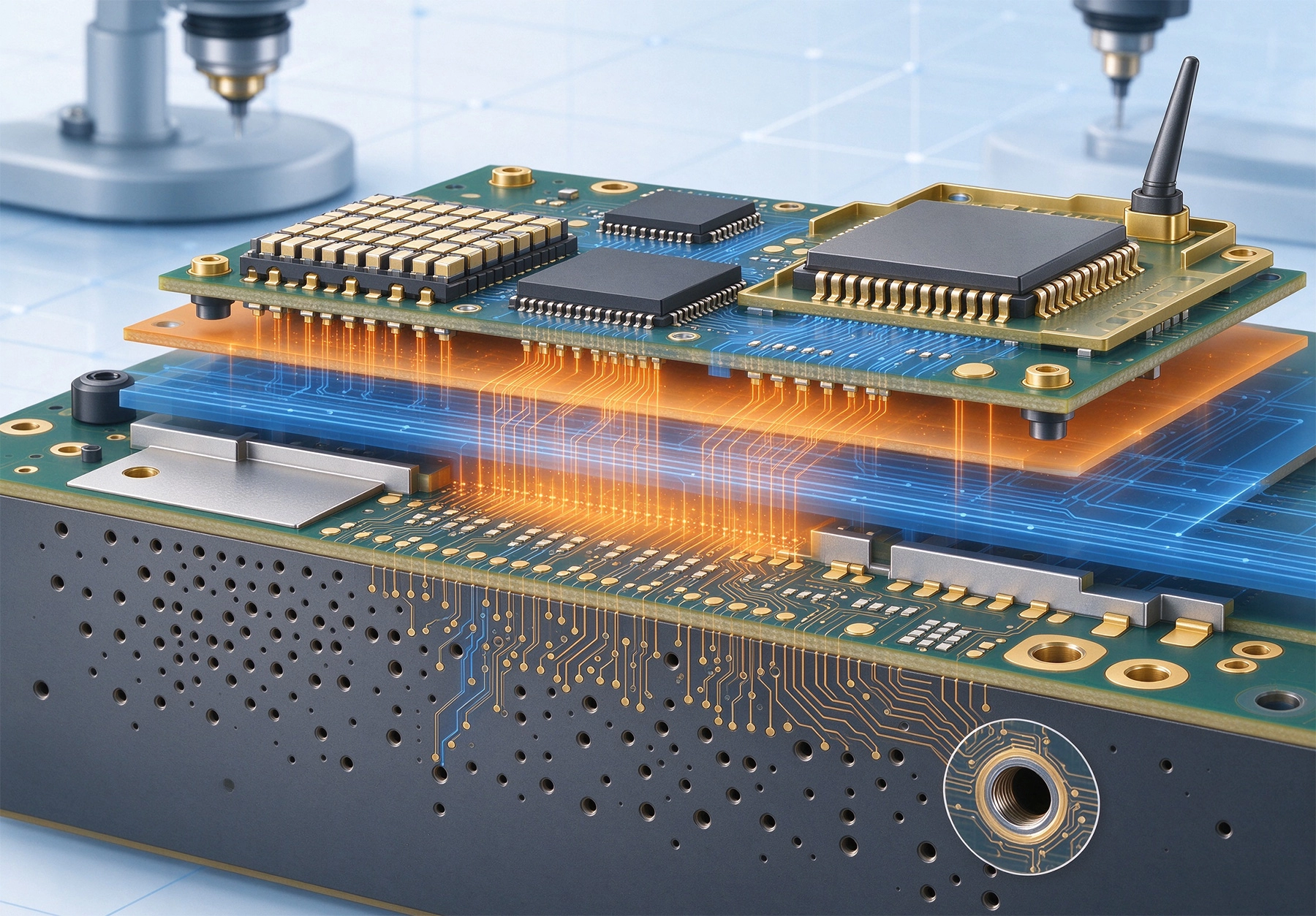
LiDAR and radar sensors operate under very different physical principles, yet both impose strict PCB requirements.
LiDAR systems typically combine high-speed digital interfaces, analog front ends, laser driver circuits, MEMS or solid-state scanning components, and precision timing modules. The PCB must carry fast data streams while maintaining clean power delivery and low-noise grounding. Vibration Resistance and thermal efficiency are also critical, because LiDAR units are often mounted in exposed vehicle locations where temperature cycling and mechanical shock are continuous.
Radar sensors, especially 77GHz and 79GHz automotive radar, are fundamentally RF devices. Their performance depends on low-loss transmission lines, precise Impedance Control, stable dielectric constants, accurate antenna geometry, and tight phase matching across antenna arrays. Any discontinuity in the PCB stack-up can distort beam patterns, reduce detection range, or increase false alarms.
HDI influences both domains, but in different ways. For LiDAR, HDI primarily improves routing density, power integrity, and mechanical robustness. For radar, HDI must be carefully combined with Low-loss Materials, because dense interconnect alone cannot compensate for poor high-frequency substrate behavior.
LiDAR modules often integrate image processors, FPGA/ASIC controllers, laser drivers, and high-speed serializers within a compact housing. HDI enables Microvias, Blind Vias, and Buried Vias that shorten signal paths between these components. Shorter paths reduce parasitic inductance and capacitance, which helps preserve signal edge quality and lowers the risk of timing errors in point-cloud data acquisition.
Laser drivers and high-performance processors demand stable, low-impedance power distribution. HDI stack-ups allow decoupling capacitors to be placed closer to IC pins through dense via fields and tighter layer transitions. This improves transient response and reduces power rail noise, which is especially important when sensitive analog receivers share the same board with high-speed digital blocks.
Automotive LiDAR must survive wide temperature cycles, continuous vibration, and long service life expectations. Hdi Boards that use filled Microvias, controlled copper thickness, and high-Tg materials can provide more reliable interconnections than traditional through-hole designs. Filled and capped vias also create flatter surfaces for fine-pitch components, reducing soldering defects and improving long-term mechanical stability.
Modern radar modules integrate multiple transmit and receive channels, high-speed digital interfaces, and complex antenna structures. HDI allows tighter routing around MMIC packages and enables more compact feed networks without expanding the board area. This is particularly important for 4D imaging radar, where channel count and data throughput are increasing rapidly.
In millimeter-wave radar, long via stubs act as resonant structures that increase Insertion Loss and cause signal reflection. HDI blind and Buried Vias reduce the need for deep through-holes, thereby shortening stub length and improving high-frequency transmission. When combined with back-drilling or optimized via placement, HDI structures help maintain cleaner S-parameters across the radar operating band.
HDI improves interconnect density, but it does not eliminate Dielectric Loss. For 77GHz radar antenna layers, Low-loss Materials such as PTFE-based laminates or ceramic-filled hydrocarbon substrates remain essential. A common approach is a hybrid stack-up: HDI routing layers for digital and control circuits, and low-loss RF layers for antenna and feed networks. This balances performance, manufacturability, and cost.
Radar feed lines and LiDAR high-speed interfaces both require controlled impedance. HDI’s thinner dielectric layers and finer traces make Impedance Control more sensitive to manufacturing variation. Line width, copper thickness, dielectric constant, and solder mask coverage must all be tightly managed. For radar systems, impedance deviation can translate directly into phase error and degraded beamforming accuracy.
Microvias shorten signal paths, but they also change the return current path. If ground references are discontinuous, HDI structures can introduce unexpected EMI or crosstalk. Continuous ground planes, closely spaced ground vias, and careful layer sequencing are essential to preserve Signal Integrity in both LiDAR and radar modules.
For radar antennas fabricated on PCB, surface flatness affects radiation patterns. HDI processes that include resin-filled vias, controlled lamination, and precise copper planarization help maintain antenna geometry. Even small variations in substrate thickness or copper profile can shift resonant frequency or distort antenna gain.
Automotive LiDAR and radar boards must survive conditions far beyond typical consumer electronics. Temperature cycling from -40°C to 125°C or higher, sustained vibration, humidity, and long operational lifetimes are standard requirements. HDI designs must therefore be evaluated not only for electrical performance but also for mechanical durability.
Filled microvias, robust Via-in-pad structures, and high-reliability surface finishes such as ENEPIG can improve resistance to thermal fatigue and corrosion. However, each additional HDI layer and laser-drilling step increases process complexity. Manufacturers must control registration accuracy, via fill quality, and lamination voids to avoid latent failures that may only appear after months of field operation.
HDI is not automatically superior for every sensor design. Higher HDI阶数 increase cost, lead time, and inspection complexity. In pure RF antenna layers, excessive via density can disturb field distribution if not carefully modeled. For very high-frequency radar, material loss, copper roughness, and phase consistency often matter more than routing density alone. The most effective designs use HDI where it improves interconnect quality, and rely on low-loss substrates and RF-aware stack-ups where electromagnetic performance is dominant.
HDI has become a foundational technology for high-performance automotive sensors. It enables shorter signal paths, denser component integration, improved power delivery, and more reliable mechanical interconnections. For LiDAR, these benefits translate into cleaner high-speed data transmission and more robust operation under vibration and thermal stress. For radar, HDI supports compact multi-channel architectures and reduced via stubs, but must be paired with low-loss materials and precise impedance control to protect RF performance. Understanding The Impact of HDI on LiDAR and Radar Sensor Performance is therefore essential for any engineer designing perception systems that must be both electrically precise and automotive-grade reliable.
No. HDI improves routing density and can reduce via stubs, but radar performance still depends heavily on substrate loss, impedance control, antenna geometry, and phase consistency. HDI should be combined with appropriate RF materials rather than used as a standalone solution.
Not always. Simple or low-channel LiDAR modules may not require advanced HDI. However, as LiDAR systems integrate more processors, faster interfaces, and smaller optical components, HDI becomes increasingly valuable for maintaining signal integrity and reducing board size.
The biggest risks are via fill quality, Layer Registration, impedance variation, and long-term reliability under thermal cycling. Automotive sensor boards require strict process control and thorough reliability testing before mass production.
The Role of IPC Standards in HDI PCB Quality AssuranceSeptember/08/2026
Conductive Anodic Filament (CAF) Resistance in High-Density BoardsJuly/31/2026
The Impact of Plating Voids on HDI Interconnect ReliabilityJuly/10/2026
Reliability Challenges of Via-in-Pad Plating Filled (VIPPO) TechnologySeptember/30/2026
Understanding and Preventing Microvia Cracking in Thermal CyclingJune/12/2026

The Role of HDI in High-Speed Server and Data Center HardwareJuly/18/2026
The Role of HDI Technology in Wearable Device MiniaturizationJuly/15/2026
Why Low Loss Materials are Critical for High-Speed HDI DesignsSeptember/01/2026