
Via-in-pad is one of those design techniques that looks deceptively simple on a schematic but carries substantial manufacturing complexity underneath. The concept is straightforward: drill a hole at a component pad location, plate it to form an electrical connection to an internal layer, fill it with a conductive or non-conductive material, cap it with copper, and use that pad for component mounting. The benefit is shorter signal paths, better electrical performance, and higher routing density — all of which matter enormously in BGA escape routing and high-speed signal design.
But the same process that enables those benefits also introduces reliability risks that are unique to Via-in-pad structures — and those risks are not always obvious from the design files. Voids in the fill, cracks in the cap plating, thermal fatigue at the fill-to-pad interface, and pad cratering under mechanical load are all failure modes that occur more frequently in via-in-pad designs than in conventional pad-over-via layouts. Understanding where these failures come from, and what process controls mitigate them, is essential for anyone designing boards that rely on VIPPO technology.
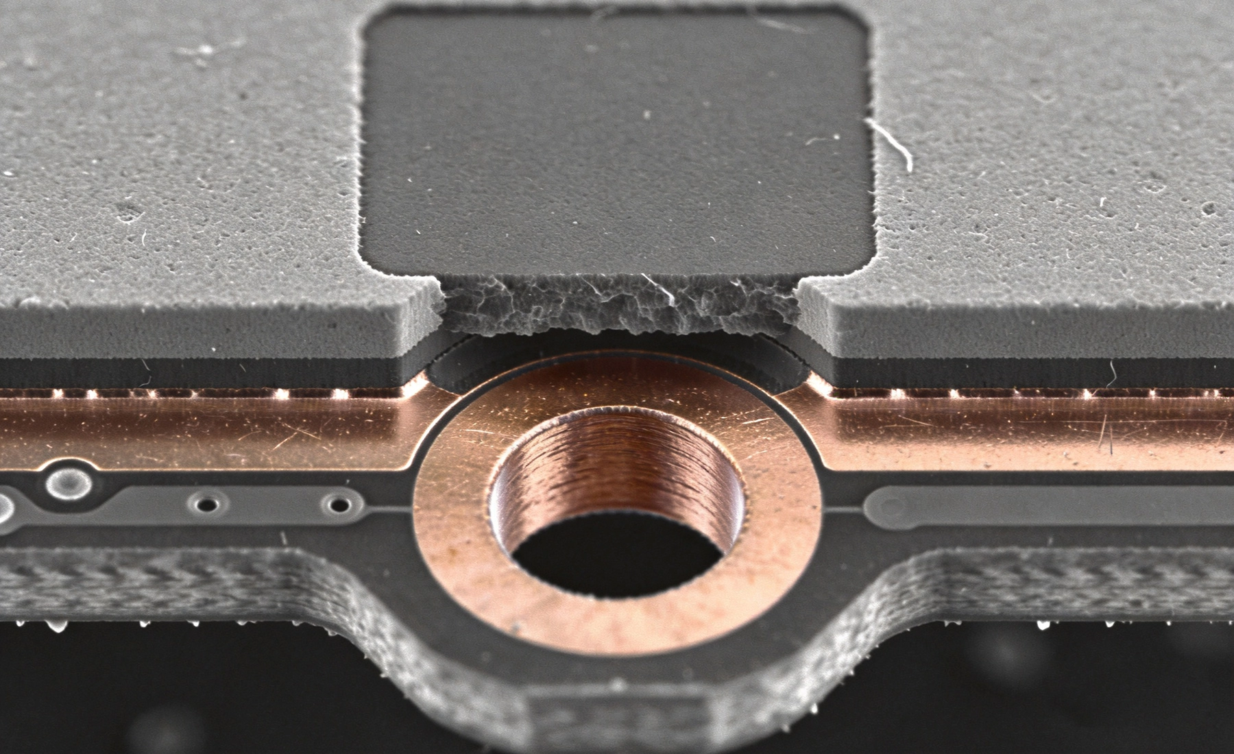
VIPPO is a specific implementation of via-in-pad where the via is filled with copper during the plating process rather than left open or filled with a non-conductive fill. The copper fill is built up by additive plating until the via barrel is completely filled with solid copper, at which point the surface is planarized and a final cap plating layer is applied to bring the pad back to the target surface finish thickness.
There are also non-conductive fill variants — where the via is filled with a polymer-based fill material after the barrel plating step — but the reliability challenges and failure modes discussed in this article focus primarily on copper-filled VIPPO structures, which are the most common in high-reliability applications and the most demanding to manufacture correctly.
The primary driver is routing density. In a high-pin-count BGA — especially at 0.4 mm pitch or finer — the number of signals that must escape the inner rows of the package often exceeds the routing channels available on the surface layer alone. Via-in-pad allows the designer to route signals from the inner BGA rows through the pad to an internal layer, where additional routing channels become available. Without via-in-pad, escaping those signals would require a larger package, more PCB layers, or a larger PCB footprint.
A secondary benefit is improved electrical performance for power and ground connections. Placing a via directly under a power or ground pad reduces the current path length and the associated inductance and resistance compared to a via placed next to the pad. For high-speed digital signals and RF applications, this reduction in via stub length and current path length has a measurable impact on Signal Integrity.
The most fundamental challenge in VIPPO manufacturing is achieving a void-free copper fill. The electroplating process that fills the via is a bottom-up growth process — copper is deposited on the sidewalls and bottom of the barrel simultaneously, and the deposit front must close at the center of the via without trapping gas bubbles or electrolyte that would create voids.
Void formation is driven by several factors: the aspect ratio of the via (depth-to-diameter ratio), the plating chemistry and current density profile, the quality of the barrier plating beneath the copper, and the surface preparation of the barrel before plating begins. High aspect ratio vias — those where the depth is significantly greater than the diameter — are the most susceptible to voiding because the electrolyte flow into the bottom of the via becomes restricted as the opening narrows during plating.
Voids in the copper fill create stress concentrators that reduce the thermal cycling performance of the structure. During temperature cycling, the coefficient of thermal expansion mismatch between the copper fill and the surrounding dielectric generates cyclic stress at the fill interface. A void near the surface of the fill acts as a crack initiation point, accelerating fatigue damage. Over hundreds or thousands of thermal cycles, a via that had a small internal void at the time of manufacture may develop a fatigue crack that opens the electrical connection.
The detection of voids requires cross-section analysis or X-ray CT scanning. Standard electrical testing on a bare board will not detect internal voids — the continuity test passes because the cap plating forms a continuous surface. Voids only become apparent when the board is cross-sectioned or when a failure occurs in the field or during thermal cycling.
After the via is filled with copper and planarized, a final cap plating layer is applied to bring the pad surface to the correct finish thickness and to provide a solderable surface. The cap plating is typically 20 to 30 micrometers of copper followed by the surface finish (ENIG, for example). This cap layer must bond uniformly to the underlying filled via without cracking.
Cap cracks are most likely to occur when there is a mismatch in the crystal orientation or grain structure between the cap plating and the underlying fill copper, or when the planarization step leaves a seam or discontinuity at the surface that propagates into the cap layer. Cracks in the cap plating can allow moisture or contamination to reach the underlying fill, creating a corrosion risk or a delamination path that propagates during thermal cycling.
From a reliability standpoint, cap cracking is particularly concerning because it is difficult to detect with standard inspection methods. AOI systems inspect the pad surface for cosmetic defects but cannot detect sub-surface cracks in the cap-to-fill interface. X-ray Inspection or cross-section analysis is required to confirm cap integrity.
Even when the fill is void-free and the cap is intact, VIPPO structures face a fundamental thermal fatigue challenge that comes from the Cte Mismatch between the copper via and the surrounding dielectric. The copper in the via expands and contracts at a different rate than the FR4 or polyimide substrate during thermal cycling, and this cyclic strain is concentrated at the interface between the fill and the pad surface.
In a conventional through-hole via, the fatigue stress is distributed along the length of the barrel. In a VIPPO structure, all the strain is concentrated at the top surface — the interface between the cap and the dielectric — because the bottom of the via is bonded to internal layers. This concentration of stress at a single interface makes the VIPPO structure more susceptible to fatigue-initiated failure than a comparable through-hole via of the same dimensions.
The practical implication is that VIPPO boards require more aggressive thermal cycling margins than standard boards to achieve the same field life. If a standard multilayer board is qualified for 1,000 thermal cycles from -40 to +125 degrees Celsius, a VIPPO board with the same thermal design may require additional qualification testing or design modifications — such as larger pad diameters or reinforced pad structures — to achieve equivalent reliability.
Pad cratering is a fracture in the PCB laminate material directly beneath the solder pad, typically caused by mechanical shock or thermal cycling. It is a well-documented failure mode in standard BGA assemblies, but VIPPO structures are more susceptible to cratering because the via fill creates a stress concentration in the laminate directly under the pad.
The filled via acts as a rigid inclusion in the flexible substrate. When the board flexes under mechanical shock or thermal stress, the strain energy concentrates at the edge of the rigid inclusion — exactly where the pad-to-laminate interface is most highly stressed. In a standard pad without a via underneath, the strain is distributed more evenly across the pad area, reducing the peak stress at any single point.
Pad cratering is particularly relevant for boards that will see mechanical shock in service — automotive under-hood applications, industrial equipment subject to vibration, or portable devices that can be dropped. The IPC-9701 standard defines the board-level drop test methods and the acceptance criteria for pad cratering evaluation.
Because VIPPO structures are typically used in Hdi Boards with Sequential Lamination, the interface between the filled via and the internal layer it connects to is a potential delamination site. The Sequential Lamination process involves applying heat and pressure to bond a new dielectric layer over a surface that already has copper features, including filled vias. If the surface preparation before lamination is inadequate — insufficient desmear, incomplete oxide treatment, or surface contamination — the bond strength at the via interface will be reduced.
Delamination at the via-to-internal-layer interface can propagate during thermal cycling or under moisture exposure, eventually causing an open circuit. This failure mode is especially concerning in boards that undergo thermal cycling during both the assembly process and the field operating life — the board experiences thermal stress twice: once during the reflow assembly and again during field operation.
The reliability risks in VIPPO structures are real and well-documented, but they are manageable with proper process controls at the manufacturing stage. Understanding what those controls are helps you evaluate a manufacturer's VIPPO capability and specify the right requirements in your design documentation.
The Copper Plating bath chemistry for VIPPO fill is typically a high-throw acid sulfate or sulfite bath formulated for bottom-up fill performance. The proprietary additives — accelerators, suppressors, and levelers — control the grain structure, growth rate, and fill behavior of the copper deposit. A manufacturer that uses well-maintained plating baths with tight process controls — regular bath analysis, additive replenishment on a time or ampere-hour basis, and documented process parameters — is more likely to produce void-free fills consistently.
Ask your manufacturer about their void rate data for VIPPO structures — the percentage of filled vias that contain voids detectable by cross-section. A manufacturer with a mature VIPPO process should be able to demonstrate void rates below 1 percent. A manufacturer that cannot provide this data, or whose data shows high void rates, may be accepting risk that will surface as field failures.
The planarization step — typically performed by CNC milling or mechanical grinding — must remove exactly the right amount of material to expose a clean, void-free fill surface without over-planarizing and exposing the underlying barrel plating. The manufacturer should use process control tools such as coplanarity measurements and Automated Optical Inspection of the planarized surface to verify that each panel meets the specification before it proceeds to the cap plating step.
For VIPPO boards, periodic cross-section analysis during production is an essential Quality Control tool. A statistical sampling plan — for example, one cross-section per panel or per lot — allows the manufacturer to verify fill quality and detect process drift before a full production lot is completed. If a cross-section reveals voids or cap cracks, the lot can be held for investigation before boards are shipped.
As a customer, you should specify in your quality plan that cross-section evidence is available upon request and that the manufacturer will notify you of any cross-section findings that indicate process anomalies.
For the most demanding applications — medical implants, aerospace systems, or other safety-critical boards — X-ray computed tomography (CT) provides the most complete non-destructive evaluation of VIPPO fill quality. CT scanning generates a 3D volumetric image of the via structure, revealing internal voids, cap cracking, and delamination that are invisible to 2D X-ray Inspection or surface inspection. While CT scanning is more expensive and slower than other methods, it provides the highest confidence in VIPPO reliability for critical applications.
Reliability is not only a manufacturing responsibility — the design decisions made before the board goes to the fab have a large impact on how reliably the VIPPO structure performs in the field.
Smaller diameter vias are more challenging to fill void-free than larger ones. At very small diameters — below 100 micrometers — the aspect ratio limits of the plating process become more constraining, and the risk of void formation increases. For designs where VIPPO reliability is a primary concern, selecting a via diameter that is at the upper end of what the routing density allows — rather than the minimum manufacturable size — improves the manufacturing margin and reduces the void risk.
For boards that will see high mechanical stress or extended thermal cycling, incorporating a reinforced pad structure — such as a captured via with a larger capture pad, or a plug-and-cap process with a secondary plating buildup — can improve the pad's resistance to cratering and fatigue. Some manufacturers offer "super burials" or reinforced VIPPO processes specifically for high-reliability applications.
The CTE of the Dielectric Material affects the magnitude of the thermal mismatch stress at the VIPPO interface. High-Tg polyimide and some ceramic-filled substrates have lower CTE values than standard FR4 and produce lower cyclic stress at the copper-dielectric interface. For boards with high thermal cycling demands, specifying a lower-CTE base material can extend the fatigue life of the VIPPO structure.
The most reliable VIPPO structure is the one that does not exist. If routing density allows, routing around the via rather than placing it in the pad eliminates all the VIPPO-specific reliability risks at once. This is not always possible — particularly in high-pin-count BGA designs — but it is worth evaluating whether every via-in-pad in the design is truly necessary or whether some could be moved to adjacent non-component areas.
For new designs that use VIPPO, a qualification test program that includes thermal cycling, thermal shock, and cross-section analysis is strongly recommended. The specific test conditions should be based on the intended application environment and the expected product lifetime.
At a minimum, a VIPPO qualification package should include:
For boards that will be exposed to mechanical shock or vibration, drop shock testing and vibration testing per IPC-9701 or the applicable MIL-STD should be added, with cross-section analysis of the VIPPO structures after testing to evaluate pad cratering resistance.
Via-in-pad plating filled technology is indispensable for high-density BGA escape routing and for achieving the routing density that modern Compact Electronics require. But it is not a risk-free design choice. The manufacturing complexity of void-free copper fill, the thermal fatigue concentration at the pad interface, and the increased susceptibility to pad cratering are reliability challenges that must be acknowledged, designed for, and controlled through process and qualification measures.
The teams that use VIPPO most successfully are those that understand the failure modes, specify the right process controls with their manufacturing partner, invest in qualification testing that probes the VIPPO structure specifically, and make design choices that give the manufacturing process adequate margin to produce reliable results. VIPPO done right is an excellent enabler of high-density design. VIPPO done without attention to the reliability fundamentals is a source of expensive field failures and customer returns.
Contact us to discuss your requirements.
Conductive Anodic Filament (CAF) Resistance in High-Density BoardsJuly/31/2026
Understanding and Preventing Microvia Cracking in Thermal CyclingJune/12/2026

The Role of IPC Standards in HDI PCB Quality AssuranceSeptember/08/2026
The Impact of HDI on LiDAR and Radar Sensor PerformanceOctober/15/2026
The Impact of Plating Voids on HDI Interconnect ReliabilityJuly/10/2026
Thermal Management Strategies for HDI Power ModulesSeptember/11/2026
Effective Thermal Management Strategies for High-Density PCBsMay/28/2026

How HDI Technology Supports Advanced Driver Assistance Systems (ADAS)June/25/2026