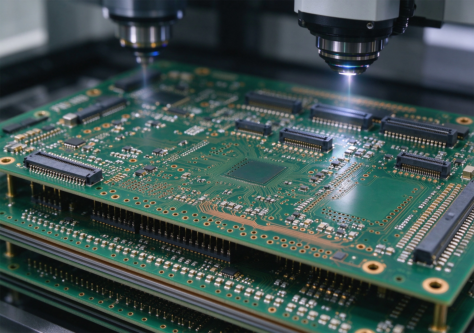
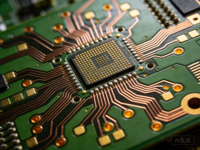
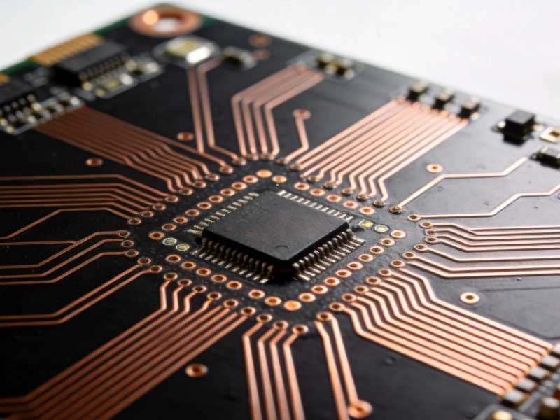
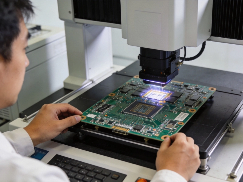
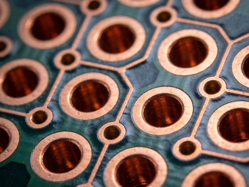
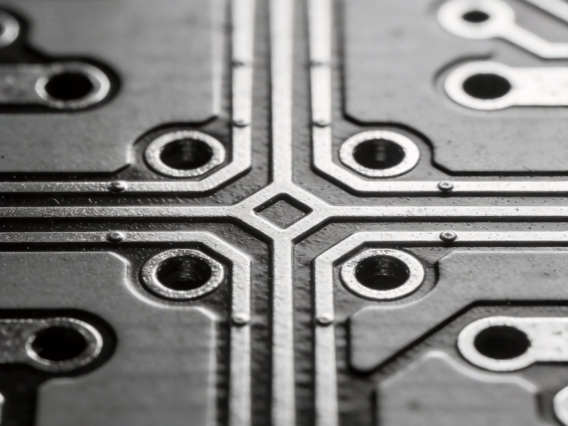
Modern networking equipment — from 400G/800G switches and routers to AI cluster interconnects and data center fabric systems — demands backplanes that can carry multi-gigabit signals across large physical distances within the chassis with minimal loss and distortion. Unlike standard PCBs, HDI (High Density Interconnect) backplanes combine fine-line routing, Microvia structures, and controlled impedance architectures to support data rates exceeding 56 Gbps per lane and approaching 112 Gbps in next-generation designs.
This guide covers the key design considerations for HDI backplanes used in high-performance networking systems, including stackup architecture, material selection, Signal Integrity, via design, power distribution, and manufacturability. It is written from the perspective of a PCBA manufacturer that regularly produces backplanes for networking and telecommunications customers.

What Makes a Backplane Different from a Standard PCB
A backplane is the central interconnect backbone of a modular system. Line cards, switch fabric cards, and power modules all plug into it. Its job is to route hundreds of high-speed differential pairs between connectors while maintaining Signal Integrity, delivering clean power, and surviving years of insertion cycles and thermal cycling.
Key differences from standard PCBs:
- Layer count: Typically 20–40 layers, sometimes exceeding 50 layers for high-port-count systems
- Board thickness: Often 4–8 mm, far thicker than standard 1.6 mm boards
- Size: Large format panels, frequently exceeding 600 × 400 mm
- Connector density: Hundreds of high-speed connectors (Ortho, Mezzanine, QSFP-DD, OSFP) mounted on a single board
- Impedance Control: Tight tolerances (±5% or tighter) across thousands of nets
- Signal integrity: Insertion Loss, return loss, crosstalk, and skew must be controlled at frequencies up to 40+ GHz
Stackup Architecture for HDI Backplanes
Layer Allocation Strategy
A well-planned stackup is the foundation of backplane performance. A typical 28–36 layer HDI backplane might allocate layers as follows:
- Signal layers: 12–20 layers dedicated to high-speed differential pairs, routed on stripline layers between reference planes
- Ground planes: Every signal layer should be bounded by solid ground planes above and below for controlled impedance and shielding
- Power planes: 4–8 layers distributed throughout the stackup to minimize impedance and provide local decoupling
- Ground shielding layers: Additional ground planes between connector rows to reduce crosstalk
The golden rule: every high-speed signal layer must have an uninterrupted reference plane. Split planes or gaps under differential pairs cause impedance discontinuities and increased EMI.
HDI Structure Options
HDI backplanes typically use one of these via structures:
- Through-hole vias only: Traditional approach for lower-speed backplanes (up to 25 Gbps); simpler manufacturing but longer via stubs cause resonance issues at higher frequencies
- Back-drilled vias: Through-hole vias with unused stub portions removed by controlled-depth drilling; extends usable frequency range to 28–56 Gbps
- Microvia + Via-in-pad: Stacked or staggered Microvias enable shorter signal paths and higher routing density; essential for 56 Gbps+ designs
- Any-layer Hdi: Microvias between any adjacent layers, enabling maximum routing flexibility; highest cost but best performance for ultra-high-density designs
For 112 Gbps PAM4 designs, Any-layer Hdi with Via-in-pad is increasingly the baseline, as stub lengths must be minimized to under 5 mils to avoid resonance within the signal bandwidth.
Material Selection for Low-Loss Performance
Dielectric Material
Standard FR-4 (Dk ≈ 4.2–4.5, Df ≈ 0.018–0.025) cannot support the Insertion Loss budgets of modern backplanes. Low-loss and ultra-low-loss laminates are required:
| Material Grade | Dk @ 10 GHz | Df @ 10 GHz | Typical Use |
|---|
| Standard FR-4 | 4.2–4.5 | 0.018–0.025 | Not suitable for 25G+ backplanes |
| Mid-loss (e.g., IS410HR) | 3.7–3.9 | 0.009–0.012 | Up to 25 Gbps |
| Low-loss (e.g., Megtron 6) | 3.7–3.8 | 0.004–0.006 | 25–56 Gbps |
| Ultra-low-loss (e.g., Megtron 7, Tachyon 100G) | 3.4–3.6 | 0.002–0.003 | 56–112 Gbps |
Material selection involves trade-offs between loss performance, cost, drillability, and availability. Megtron 6 has been the workhorse for 56 Gbps backplanes; Megtron 7 and Tachyon 100G are gaining adoption for 112 Gbps designs. Always verify material availability with your fabricator early in the design cycle, as lead times for specialty laminates can be 4–6 weeks.
Copper Foil Type
At high frequencies, current flows primarily on the conductor surface (Skin Effect). Surface roughness significantly impacts insertion loss:
- Standard ED foil: Rough surface, higher loss — avoid for high-speed layers
- Reverse-treated foil (RTF): Smoother surface, moderate improvement
- Very-low-profile (VLP) foil: Rz ≤ 2 µm, recommended for 25 Gbps+ signal layers
- Ultra-low-profile (ULP/HVLP) foil: Rz ≤ 1 µm, preferred for 56 Gbps+ designs
Using HVLP copper on signal layers can reduce insertion loss by 10–20% compared to standard foil — equivalent to gaining several inches of trace length within the same loss budget.
Signal Integrity Design
Impedance Control
Backplane impedance targets are typically:
- Single-ended: 50 Ω ± 5%
- Differential: 85 Ω, 90 Ω, 100 Ω, or 120 Ω depending on the connector and protocol standard (±5% or tighter)
Achieving tight Impedance Control on thick, multi-layer boards requires:
- Precise control of dielectric thickness between signal and reference planes
- Consistent copper thickness and etch factor across the panel
- Impedance test coupons on every panel, measured with Tdr
- Close collaboration with the fabricator on stackup design before finalizing layout
Insertion Loss Budget
For a 112 Gbps PAM4 channel, the total insertion loss budget from ASIC to ASIC is typically 30–35 dB at 28 GHz (Nyquist frequency). This budget must be allocated across:
- Package and substrate: ~4–6 dB
- Daughter card trace: ~3–5 dB
- Connector (two interfaces): ~4–6 dB
- Backplane trace: ~12–18 dB
This means backplane traces must be kept as short as possible, and the material must deliver very low loss. For a 300 mm trace on Megtron 7, insertion loss at 28 GHz is approximately 10–12 dB — within budget. The same trace on standard FR-4 would exceed 25 dB, making the link non-functional.
Crosstalk Management
With hundreds of differential pairs routed in parallel, crosstalk is a major concern:
- Spacing: Maintain ≥ 3× trace width between differential pairs (5× preferred for critical nets)
- Ground stitching: Place ground vias between connector pin rows and along signal routes
- Layer assignment: Route orthogonal directions on adjacent signal layers to reduce broadside coupling
- Guard traces: Use grounded guard traces between critical pairs where spacing is insufficient
- Length matching: Match intra-pair skew to ≤ 5 mils and inter-pair skew to ≤ 10 mils within a bus
Via Design and Backdrilling
Via Stub Problem
A through-hole via on a 5 mm thick backplane has a stub (the unused portion beyond the target layer) that acts as a resonant antenna. At 28 GHz, a stub longer than ~2.5 mm creates a quarter-wave resonance that severely degrades the signal. Solutions:
- Backdrilling: After through-hole plating, drill out the unused stub portion from the opposite side. Residual stub should be ≤ 8 mils for 56 Gbps and ≤ 5 mils for 112 Gbps.
- Microvias: Blind or buried microvias eliminate stubs entirely by connecting only the required layers.
- Via-in-pad: Places the via directly in the component pad, minimizing the transition length; requires Via Filling and plating over for reliable assembly.
Backdrilling Design Guidelines
- Specify the backdrill depth tolerance (typically ±0.1 mm) on fabrication drawings
- Ensure ≥ 0.2 mm clearance between the backdrill barrel and surrounding copper to avoid shorting
- Avoid routing signals on layers that would be removed by backdrilling
- Use teardrop pads at via entries to reduce stress concentration
- Mark backdrilled vias with a unique drill symbol in the fabrication drawing
Power Distribution Network (PDN)
Modern networking ASICs draw hundreds of amps at sub-1V core voltages. The backplane PDN must deliver clean, stable power:
- Power plane pairs: Use closely spaced power-ground plane pairs (≤ 0.1 mm separation) to create inherent inter-plane capacitance
- Low-impedance target: PDN impedance should be ≤ 1 mΩ from DC to several hundred MHz
- Distributed decoupling: Place bulk, mid-frequency, and high-frequency capacitors near each connector and power entry point
- Via fencing: Use multiple vias per power pin to reduce inductance; 4–8 vias per power connection is common
- IR drop analysis: Simulate DC voltage drop across the backplane to ensure all loads receive adequate voltage under worst-case current
Thermal and Mechanical Considerations
Thermal Management
Backplanes dissipate significant heat from connectors, termination resistors, and power distribution:
- Use thermal relief vias to conduct heat from hot spots to internal copper planes
- Maintain airflow channels between connector rows aligned with the system cooling architecture
- Avoid placing thermally sensitive components (precision resistors, crystals) near high-power areas
- Consider Thermal Simulation during design to identify hot spots before prototyping
Mechanical Robustness
Backplanes undergo repeated card insertion and removal over their service life:
- Press-fit connectors: Require precise hole size control (typically ±0.025 mm) and sufficient copper barrel thickness to withstand insertion forces
- Board stiffness: Thick backplanes are inherently rigid, but large boards may need stiffeners or support rails to prevent warpage
- Connector mounting: Use through-hole mounting pins with adequate pad size and solder fillets for mechanical strength
- Warpage control: Specify warp ≤ 0.5% for reliable press-fit assembly; symmetric stackup design is critical
Manufacturing and Quality Control
Fabrication Challenges
- Registration: Aligning 30+ layers within ±0.075 mm requires precision lamination and optical alignment systems
- Impedance control: Requires tight process control on dielectric thickness, copper etching, and lamination pressure
- Backdrilling depth accuracy: Needs specialized equipment and process control
- Via Filling: Via-in-pad structures require epoxy filling and Copper Plating over for reliable soldering
- Panel utilization: Large backplanes may be built as single-up panels, increasing cost; design for panelization where possible
Testing and Inspection
- 100% electrical testing: Flying probe or fixture-based testing for opens and shorts
- Tdr impedance verification: Measure impedance on test coupons and critical nets
- X-ray Inspection: Verify via fill quality, voiding, and press-fit hole integrity
- Microsectioning: Cross-section samples to verify via plating thickness, lamination quality, and backdrill depth
- Time-domain and frequency-domain testing: Vector network analyzer (VNA) measurements on sample boards to validate insertion loss, return loss, and crosstalk
Summary Checklist for HDI Backplane Design
- ☐ Low-loss or ultra-low-loss laminate selected (Megtron 6/7, Tachyon, etc.)
- ☐ HVLP copper foil on high-speed signal layers
- ☐ Stackup designed with solid reference planes for every signal layer
- ☐ Impedance targets defined and verified with fabricator
- ☐ Via stubs eliminated via backdrilling or microvias
- ☐ Differential pair spacing ≥ 3× trace width with ground stitching
- ☐ Intra-pair skew ≤ 5 mils, inter-pair skew ≤ 10 mils
- ☐ PDN designed for ≤ 1 mΩ impedance with distributed decoupling
- ☐ Thermal and mechanical analysis completed
- ☐ Backdrilling and via-in-pad requirements clearly specified in fabrication drawings
- ☐ Test strategy defined: TDR, VNA, X-ray, microsection
- ☐ Fabricator engaged early for DFM review
Designing an HDI backplane for high-performance networking equipment is one of the most demanding tasks in PCB engineering. It requires deep collaboration between signal integrity engineers, layout designers, and fabricators — and every decision, from material selection to via geometry, directly impacts whether the system can achieve its target data rate. The boards that succeed are those where simulation, design discipline, and manufacturing capability are aligned from day one.