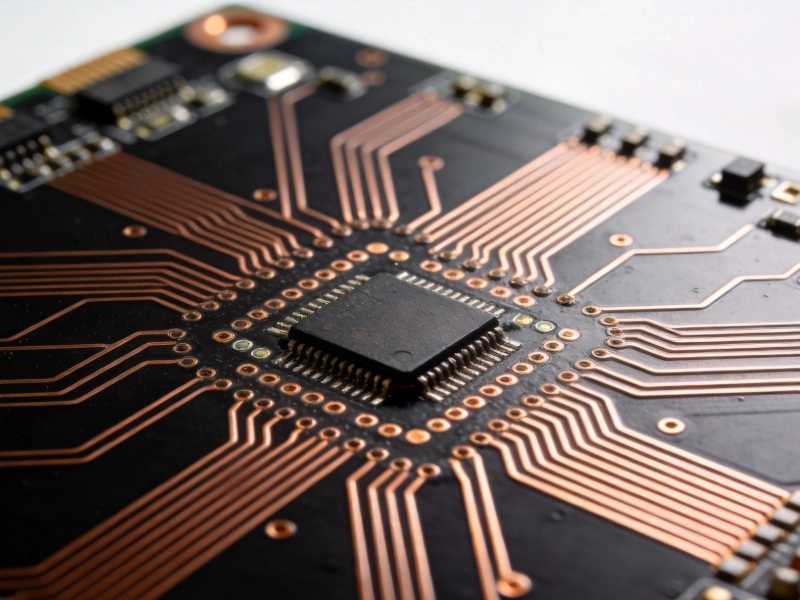
The semiconductor industry keeps shrinking feature sizes while packing more functionality into each chip. The result: Ball Grid Array packages with pitches of 0.4mm, 0.3mm, and even 0.2mm, mounted on HDI substrates that route signals through Microvias and fine traces. This combination delivers remarkable Miniaturization—but it creates testing challenges that keep manufacturing engineers up at night.
When you can't see the solder joints, how do you know they're good? When standard test probes won't fit, how do you verify functionality? When traditional inspection methods fail, what alternatives exist? This guide addresses the testing and inspection challenges of fine-pitch BGA on HDI, and the solutions that help ensure reliability.

Understanding Fine-Pitch BGA and HDI Technology
Before diving into testing challenges, let's clarify what we're dealing with. The combination of fine-pitch BGA and HDI represents the cutting edge of Electronics Packaging.
What is Fine-Pitch BGA?
Ball Grid Array packages mount chips face-up or face-down on a substrate, with connections made through an array of solder balls on the package bottom. The pitch—the distance between ball centers—determines how much I/O can fit in a given package size.
- Standard pitch BGA: 1.0mm, 0.8mm, 0.65mm pitch—established technology, relatively straightforward testing
- Fine-pitch BGA: 0.5mm, 0.4mm, 0.35mm pitch—challenging but manageable with care
- Ultra-fine-pitch BGA: 0.3mm, 0.25mm, 0.2mm pitch—requires advanced techniques and specialized equipment
As pitch decreases, the solder joint height decreases proportionally. This means less tolerance for variation in paste volume, placement accuracy, and reflow dynamics. A defect that would cause an open circuit in standard pitch becomes catastrophic at ultra-fine pitch.
What is HDI PCB Technology?
High-density Interconnect (HDI) PCBs use Microvias (typically ≤0.15mm diameter) and finer trace widths to achieve higher routing density than standard multilayer boards. Common HDI structures include:
- 1-N-1 structure: One layer of microvias between outer layers and the next inner layer
- Any-layer Hdi: Any layer can connect to any other layer through microvias, enabling ultra-high density
- Build-up layers: Thin dielectric layers with sequential Microvia formation
HDI enables fanout from fine-pitch BGAs where standard Pcb Technology can't route the signals. But HDI substrates also have different thermal and mechanical properties than traditional boards—properties that affect solder joint reliability.
Why Testing Becomes Critical
Fine-pitch BGA on HDI creates a compounding effect of challenges:
- Invisible joints: BGA solder joints are hidden beneath the package; nothing is visible for inspection
- Tiny features: Microvias and fine traces require precise process control
- Thermal mismatch: Different expansion coefficients between BGA, substrate, and PCB create reliability concerns
- Limited accessibility: Test access points may be impossible to place near the BGA
For consumer electronics, some defects may be acceptable given product lifetime expectations. For medical devices, automotive safety systems, or Aerospace Electronics, zero defects may be required. Testing strategy must match application requirements.
The Core Testing Challenges
Fine-pitch BGA on HDI creates specific testing challenges that require specialized approaches.
Challenge 1: Physical Inaccessibility
The BGA package covers its own solder joints. By design, there's no physical access to the connection points between the package and the PCB. This creates several problems:
- No probe access: Standard in-circuit test fixtures can't reach joints under the package
- Limited visual inspection: Even with magnification, solder joints aren't visible
- No probe repair: If a probe touches a joint during testing, it damages the joint
Challenge 2: Thermal Profile Sensitivity
Fine-pitch BGA solder joints are more sensitive to thermal excursions than larger joints. Temperature variations during testing can affect results:
- Temperature cycling: Testing at extreme temperatures may cause joint stress
- Self-heating: Powered boards generate heat that affects measurements
- Reflow effects: Repeated thermal exposure can degrade joint integrity over time
Challenge 3: Signal Integrity at Fine Pitch
High-speed signals passing through fine-pitch BGAs face additional concerns:
- Impedance Control: Variations in pad size, via stub length, and routing affect impedance
- Crosstalk: Dense Bga Routing increases coupling between signals
- Power integrity: Power delivery to fine-pitch BGAs requires careful PDN design
Challenge 4: HDI Substrate Brittleness
HDI substrates, with their thin dielectric layers and microvias, can be more sensitive to mechanical stress:
- Via reliability: Microvias in HDI are more susceptible to stress than through-hole vias
- Pad adhesion: Fine-pitch pads may have less pull strength than larger pads
- Flexure sensitivity: Some HDI substrates are designed for rigid applications only
Inspection Technologies for BGA
Since direct physical inspection of BGA joints is impossible, alternative inspection technologies have evolved to provide visibility into solder joint quality.
X-Ray Inspection Systems
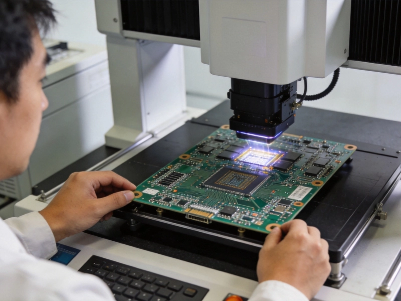
X-ray Inspection is the primary method for examining hidden BGA solder joints. Different technologies offer different capabilities.
2D X-Ray Systems
- Principle: X-rays pass through the board; density variations create contrast in the image
- Best for: Detecting gross defects, missing balls, gross voiding
- Limitations: Overlapping features appear superimposed; depth information limited
3D X-Ray/CT Systems
- Principle: Multiple X-ray images are combined to create a volumetric reconstruction
- Best for: Precise void analysis, crack detection, precise joint inspection
- Limitations: Slow; expensive; limited for production-line speeds
Laminography Systems
- Principle: Focal plane tomography that images a specific layer while rejecting out-of-focus information
- Best for: Layer-by-layer inspection of BGA joints; faster than CT for some applications
- Limitations: Complex setup; requires expertise to interpret
When inspecting BGA joints, engineers evaluate:
- Void percentage: Voids in solder reduce joint strength; typically limited to 25% or less of joint area
- Joint shape: Ideal joint is cylindrical with slight hourglass shape; spherical or collapsed joints may indicate problems
- Solder fill: Complete fill of the BGA pad and component pad is essential
- Cracks: Cracked joints may not be visible until 2D X-ray; CT may be required
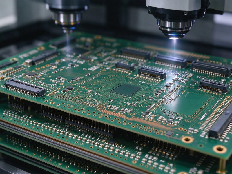
Automated Optical Inspection (AOI) Limitations
AOI is highly effective for visible solder joints, but has fundamental limitations for BGAs:
- Cannot see under the package: AOI can only inspect what it can see
- Co-planarity inspection: AOI can verify BGA ball co-planarity before reflow
- Post-reflow limitations: After reflow, only package shadow is visible
AOI is valuable for:
- Inspecting other joints on the board (QFP, QFN, connectors)
- Verifying component placement accuracy before reflow
- Detecting gross defects like tombstoning or misplacement
Acoustic Microscopy (C-SAM)
Scanning Acoustic Microscopy uses ultrasonic waves to detect internal features:
- Best for: Detecting delamination, cracks, voids in solder joints
- How it works: Sound waves reflect at material interfaces; variations indicate defects
- Limitations: Cannot detect fine cracks in solder; limited resolution for small voids
In-Circuit Testing Approaches
In-circuit test verifies that each component is present and correctly installed. For boards with BGAs, traditional ICT has limitations, but several approaches can help.
Boundary Scan (JTAG) Testing
Boundary scan is the most powerful ICT approach for BGA-heavy boards. JTAG (Joint Test Action Group) technology embeds test circuitry into ICs, allowing test access through standard test points.
How Boundary Scan Works
- Test access port: ICs with boundary scan have dedicated test pins (TCK, TMS, TDI, TDO)
- Shift register chain: Test data shifts through boundary scan cells surrounding each I/O
- Control capability: Can force values at pins and observe responses without physical access
Boundary Scan Advantages
- Tests BGAs without physical probe access to joints
- Detects opens, shorts, and incorrect component values
- IEEE 1149.1 standard ensures broad tool and component support
- Effective for digital logic and many mixed-signal devices
Boundary Scan Limitations
- Requires ICs with boundary scan capability
- Cannot directly test passive components between non-scan devices
- Analog circuits may not be fully testable
- Setup and programming require expertise
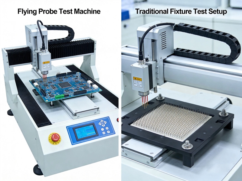
Flying Probe Testing
Flying probe systems use programmatically positioned probes rather than fixed beds:
- Flexibility: Can probe anywhere on the board; ideal for prototypes and low volumes
- No fixture cost: Eliminates expensive bed-of-nails fixtures
- Limitation: Slower than dedicated fixtures; not practical for high-volume production
For BGA testing, flying probe can access:
- Test points on the PCB (even if near the BGA)
- Component leads accessible from the board edge
- Power and ground planes for current measurements
Bed-of-Nails Fixtures with Strategic Access
For high-volume production, dedicated fixtures with strategic probe placement can achieve good coverage:
- Test points: Add test points to the Pcb Design specifically for ICT access
- Via targets: Some designs allow probing vias near (but not on) BGA joints
- Connector access: Test through connectors where possible
The limitation: many defects will still be invisible to ICT because they occur at joints that can't be accessed.
Functional Testing Strategies
Functional testing verifies that the board performs its intended function—not just that components are correct. For BGA-heavy boards, functional test is essential because ICT cannot catch all defect types.
Board-Level Functional Test
- Power-on test: Verify the board powers up without excessive current draw
- Boot verification: For processor boards, verify boot code executes
- Interface testing: Exercise communication interfaces to verify functionality
- Boundary scan functional: Use boundary scan to exercise internal logic paths
Stress Testing and Burn-In
Some Bga Defects only appear under stress conditions:
- Thermal cycling: Temperature extremes can reveal marginal joints
- Power cycling: Repeated power on/off exposes thermal fatigue issues
- Burn-in: Extended operation at elevated temperature accelerates failure of marginal joints
Boundary Scan for Functional Test
Advanced boundary scan implementations can perform functional-like testing:
- Memory testing: Write and read patterns through scan-accessible memory
- Flash programming: Program flash memory via boundary scan to verify data path
- Logic test patterns: Apply test vectors through boundary scan to exercise logic
Design for Testability (DFT)
The best testing strategy starts with design decisions. Designing for testability from the beginning costs far less than retrofitting testability later.
Test Access Point Placement
Design your PCB with testing in mind:
- JTAG connector: Include a connector for boundary scan access; make it accessible
- Test points: Add test points near critical nets, especially power and ground
- Switchable probes: Consider adding switches or jumpers that allow probe access only during test
- Via farming: Group vias in testable areas rather than spreading them across the board
Boundary Scan Chain Design
Design your boundary scan implementation for testability:
- Single chain: Connect all boundary scan devices in a single chain for simplicity
- Clear TAP routing: Route JTAG signals to allow easy probe connection
- Enable signals: Make boundary scan enable signals controllable and observable
- Pre-layout planning: Plan boundary scan chain before layout begins
Diagnostic Header Design
Add features that support diagnostics:
- LED indicators: Power good, fault indicators
- Debug headers: Serial interfaces for software diagnostics
- Reset controls: Ability to reset sections of the board
- Voltage monitors: Test points for key power rails
Defect Detection Capabilities
Understanding what each test method can and cannot detect helps optimize your test strategy.
What X-Ray Detects
- Detects well: Voids, missing balls, misalignment, gross solder defects
- Detects partially: Microcracks, subtle joint quality issues
- Cannot detect: Cold joints (sufficient solder but poor metallurgy), subtle opens
What ICT Detects
- Detects well: Wrong components, wrong values, opens on accessible nets, shorts between probed nodes
- Detects partially: Some joint issues if they cause measurable resistance changes
- Cannot detect: Most BGA joint defects, unless they cause the net to be completely open
What Functional Test Detects
- Detects well: Boards that don't function; interface failures; gross electrical issues
- Detects partially: Margins issues that cause intermittent failures
- Cannot detect: Defects that don't manifest during test (latent defects)
What Burn-In Detects
- Detects well: Marginal joints that fail under thermal or power stress
- Detects partially: Early-life failures before they reach customers
- Cannot detect: Defects that require longer stress exposure
Building an Effective Test Strategy
No single test method catches all defects. The most effective approach combines multiple methods in a strategy matched to your reliability requirements and production volume.
Test Pyramid Approach
A layered test strategy provides comprehensive coverage:
- Design verification: First articles, DFM analysis, prototype testing
- Screening tests: AOI, Axi, ICT—high throughput, catch obvious defects
- Functional tests: Board-level functional verification
- Stress tests: Burn-in, thermal cycling for high-reliability applications
Risk-Based Testing
Match test intensity to risk level:
- High-reliability applications: Comprehensive testing including X-ray inspection, ICT, functional test, and burn-in
- Consumer electronics: Screening tests plus basic functional test may suffice
- Prototypes: Full inspection and testing to identify design issues before production
Volume Considerations
- High volume: Invest in dedicated fixtures, automated inspection, and efficient test cells
- Medium volume: Flexible test equipment, flying probe, and selective inspection
- Low volume/prototype: Manual inspection, flying probe, extensive functional testing
Working with Your CM on BGA Testing
Your contract manufacturer plays a critical role in BGA testing. Choose partners with appropriate capabilities and establish clear expectations.
What to Look For in a CM
- X-ray capability: Appropriate X-ray inspection equipment for your BGA types
- Boundary scan expertise: Ability to implement and debug boundary scan tests
- Test fixture capability: In-house fixture building or trusted vendors
- DFT consultation: Willingness to review your design for testability
- Documentation: Willingness to provide first-article inspection reports
Questions to Ask
- What X-ray inspection capability do you have? What pitch BGAs have you tested?
- What's your approach for BGA boards without boundary scan ICs?
- What defect escape rate do you target?
- Do you provide first-article inspection reports?
- What's your test coverage for BGA joints specifically?
Common BGA Defects and Their Detection
Open Joints
Opens occur when solder fails to form a complete connection:
- Causes: Insufficient solder, poor wetting, component lift during reflow
- Detection: X-ray can see some opens; boundary scan can detect some; many escape
Bridging/Shorting
Bridging occurs when solder connects adjacent joints:
- Causes: Excess paste, component shift, contamination
- Detection: X-ray can see bridges; ICT can detect shorts; functional test may detect shorts
Voiding
Voids are gas pockets in the solder joint:
- Causes: Outgassing during reflow, moisture in components, process issues
- Detection: X-ray detects voids easily; percentage voiding is measurable
Head-in-Pillow
Head-in-pillow occurs when the BGA ball and paste don't fully merge:
- Causes: Oxidation, uneven heating, warpage
- Detection: X-ray may show partial connection; may pass ICT but fail under stress
- Risk: Intermittent failures that escape testing
Pad Cratering
Pad Cratering occurs when the PCB pad delaminates from the substrate:
- Causes: Mechanical stress, thermally induced stress, poor laminate adhesion
- Detection: Often only detectable via cross-sectioning or acoustic microscopy
Conclusion
Testing fine-pitch BGA on HDI represents one of the most challenging areas of Electronics Manufacturing. The combination of invisible joints, tiny features, thermal sensitivity, and limited accessibility requires a comprehensive approach that combines multiple testing technologies.
No single test method catches everything. X-ray inspection reveals internal joint quality. Boundary scan provides access without physical probing. Functional testing verifies that the board actually works. Burn-in catches marginal joints before they fail in the field. The right combination depends on your specific requirements for reliability, cost, and volume.
The most effective strategy starts with design. Designing for testability—adding test points, including boundary scan, planning for inspection access—costs far less than compensating for poor testability later. Work with your manufacturing partners early in the design process to ensure your products can be tested effectively.
As BGA pitches continue decreasing and HDI complexity increasing, testing challenges will only grow. Staying current with inspection technologies, boundary scan capabilities, and test methodologies is essential for companies building advanced electronics. The investment in test capability pays dividends in quality, reliability, and reduced field failures.
Frequently Asked Questions
Can X-ray inspection detect all BGA defects?
No. X-ray can detect voiding, misalignment, missing balls, and some bridging, but it cannot reliably detect head-in-pillow defects, subtle cracks, or cold joints where the connection appears adequate but has poor metallurgy. A comprehensive test strategy combining X-ray, ICT, boundary scan, and functional testing provides the most complete coverage.
What's the minimum BGA pitch that can be reliably tested?
Modern X-ray systems can inspect BGAs down to 0.2mm pitch and below. However, inspection resolution and reliability improve at larger pitches. At ultra-fine pitch (below 0.3mm), inspection becomes more challenging and defect detection reliability decreases. Consult with your CM about their specific capabilities.
Is boundary scan testing required for BGA boards?
Boundary scan is highly recommended for BGA-heavy boards because it provides access to internal nodes that physical probing cannot reach. However, it requires that ICs support boundary scan (IEEE 1149.1). If your design doesn't include boundary scan devices, ICT and functional testing become more critical to compensate for the loss of this capability.
How much does BGA testing add to manufacturing cost?
Testing costs vary widely based on volume, complexity, and defect rate requirements. X-ray inspection typically adds 5-15% to assembly cost depending on coverage. Boundary scan development adds NRE cost but reduces per-unit cost at volume. For high-reliability applications where field failures are costly, testing investment is justified by reduced failure costs.
What's the difference between AXI and AOI for BGA inspection?
AOI (Automated Optical Inspection) cannot see under the BGA package and is limited to pre-reflow inspection of ball co-planarity and placement. Axi (Automated X-ray Inspection) uses X-rays to see through the package and inspect solder joints themselves. AXI is the primary production inspection method for BGAs; AOI supplements by inspecting visible joints elsewhere on the board.
Need help developing a test strategy for your fine-pitch BGA boards? Our engineering team can review your design and recommend appropriate testing approaches.