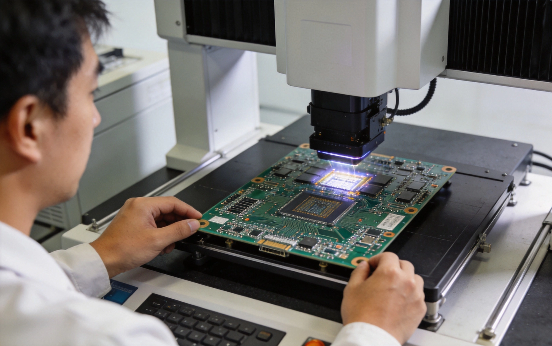
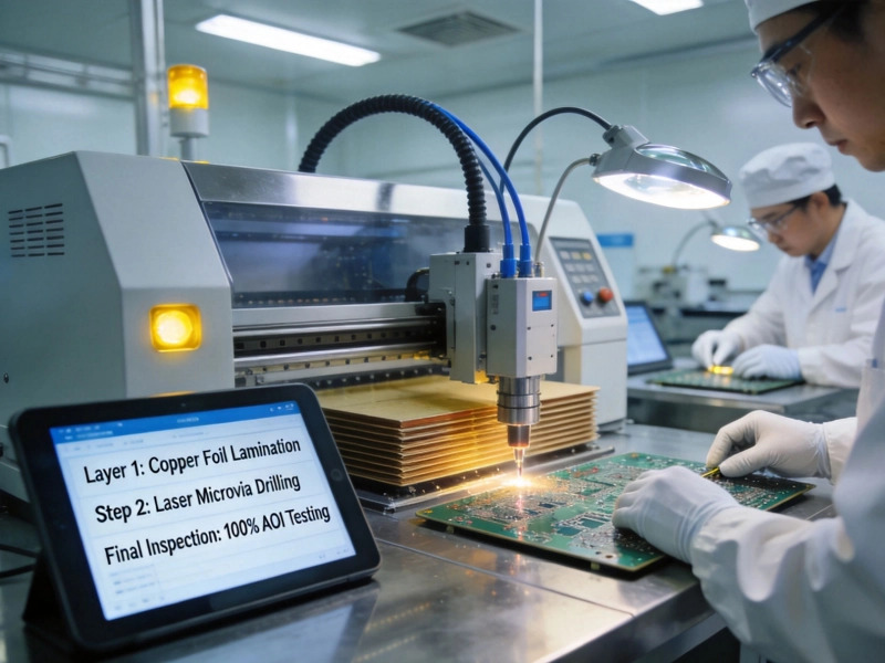
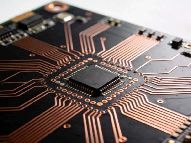
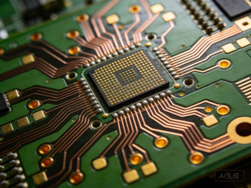
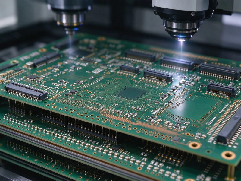
Multilayer High-density Interconnect (HDI) PCBs form the foundation of modern compact, high-performance electronics including smartphones, medical implants, aerospace systems, and automotive advanced Driver Assistance Systems. With trace widths as small as 25μm, Microvias (blind, buried, and stacked), and layer counts ranging from 8 to 30+, Hdi Boards feature extremely complex internal structures that are impossible to inspect with traditional visual methods alone. Non-Destructive Testing (NDT) techniques allow manufacturers to evaluate internal quality, detect Hidden Defects, and validate reliability without damaging these high-value circuit boards, making NDT an essential part of HDI Pcb Quality Control.

Unique Inspection Challenges of Multilayer HDI PCBs
The compact, layered design of HDI PCBs creates significant inspection challenges that require specialized NDT solutions:
-
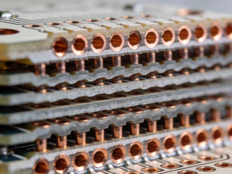
Hidden Internal Structures: Most critical features including Buried Vias, inner layer traces, and interlayer connections are completely hidden from external view, making visual inspection useless for internal defect detection.
-
Miniaturized Features: Microvias as small as 50μm in diameter and fine-pitch components require extremely high-resolution inspection capabilities to detect minute defects.
-
High Manufacturing Cost: Multilayer HDI PCBs are significantly more expensive to produce than standard PCBs, so destructive testing that results in scrapped units is economically impractical.
-
Complex Defect Modes: Common HDI defects such as incomplete Via Filling, interlayer delamination, misaligned layers, and hidden solder joint failures cannot be detected through standard electrical testing alone.
-
Critical Reliability Requirements: HDI PCBs are often used in safety-critical applications where even minor defects can lead to catastrophic failures, requiring 100% inspection coverage.
Core Non-Destructive Testing Techniques for HDI PCBs
Modern Hdi Manufacturing uses a combination of complementary NDT techniques to provide comprehensive defect coverage across all production stages:
1. X-Ray Inspection (2D and 3D)
X-ray Inspection is the most widely used NDT technique for multilayer HDI PCBs, as X-rays can penetrate all layers of the board to reveal internal structures:
-
2D X-Ray: Provides fast, high-resolution imaging of internal features to detect incomplete Via Filling, solder bridges, missing components, BGA solder joint defects, and foreign objects embedded between layers.
-
3D X-Ray (Computed Tomography / CT): Constructs a full 3D model of the PCB by combining hundreds of X-ray images taken from different angles, allowing precise detection of complex defects such as stacked via misalignment, hidden solder voids, inner layer short circuits, and trace cracks in internal layers. Modern CT systems can achieve resolution down to 1μm, making them ideal for the smallest HDI features.
X-ray Inspection is particularly critical for
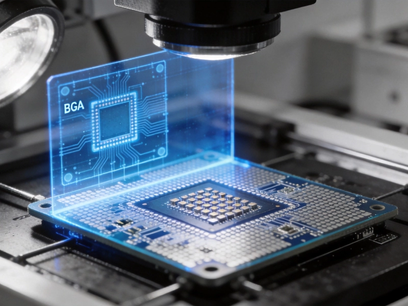
Hdi Boards with BGA, CSP, or flip-chip components, where solder joints are completely hidden under the component package.
2. Automated Optical Inspection (AOI)
AOI uses high-resolution cameras, advanced lighting systems, and AI-powered image analysis to inspect visible surfaces of HDI PCBs:
-
Detects surface defects including solder bridges, open solder joints, component misalignment, missing components, tombstoning, and trace damage on outer layers.
-
Operates at high speeds, making it suitable for in-line inspection during production.
-
Advanced AOI systems with 12+ megapixel cameras and 3D scanning capabilities can detect even the smallest defects on fine-pitch HDI components.
While AOI cannot inspect internal layers, it provides fast, cost-effective detection of surface defects at multiple stages of the manufacturing process.
3. Scanning Acoustic Microscopy (SAM)
Scanning Acoustic Microscopy uses high-frequency ultrasound waves to detect defects at material interfaces that X-rays may miss:
-
Identifies interlayer delamination, voids in prepreg or adhesive layers, and moisture-induced separation between PCB layers.
-
Detects defects in solder joint interfaces, including cracks and voids that may lead to reliability failures under thermal cycling.
-
Particularly valuable for reliability testing, as it can detect latent defects that would only appear after the board is exposed to operational stresses.
SAM is especially important for HDI PCBs used in high-temperature or high-vibration environments, where delamination is a common failure mode.
4. Infrared (IR) Thermography
Infrared thermography uses thermal cameras to detect temperature variations across the PCB when powered:
-
Identifies hidden short circuits, high-resistance connections, and component failures by detecting abnormal hot spots.
-
Can detect defects in internal power planes that would otherwise require destructive cross-sectioning to locate.
-
Non-contact and fast, making it suitable for screening large numbers of boards for functional defects.
IR thermography is often used in combination with electrical testing to locate the source of electrical faults without damaging the board.
5. Terahertz (THz) Imaging
Terahertz imaging is an emerging NDT technology that uses low-energy terahertz radiation to penetrate Pcb Materials:
-
Provides excellent contrast between different Pcb Materials, allowing detection of delamination, voids, and thickness variations in internal layers.
-
Does not use ionizing radiation, making it safer for operators than X-ray systems.
-
Particularly effective for inspecting thick multilayer HDI boards where X-ray penetration may be limited.
As terahertz technology continues to improve and become more affordable, it is expected to play an increasingly important role in
Hdi Pcb inspection.
6. Time-of-Flight Secondary Ion Mass Spectrometry (ToF-SIMS)
ToF-SIMS is a highly sensitive surface analysis technique used for specialized HDI testing:
-
Detects surface contamination, plating thickness variations, and material composition issues that can lead to solderability or reliability problems.
-
Can analyze both organic and inorganic materials at the molecular level, making it ideal for failure analysis of Hdi Reliability issues.
While not used for routine production inspection, ToF-SIMS is invaluable for root cause analysis when field failures occur.
Selecting the Right NDT Combination for Your HDI Project
The optimal NDT strategy depends on your specific HDI design, application, and risk profile:
-
Low-Consumer Electronics: Combination of AOI for surface inspection and 2D X-ray for BGA and via inspection provides sufficient coverage at reasonable cost.
-
Automotive and Industrial Applications: Add SAM inspection to detect potential delamination issues that could cause failures under harsh operating conditions.
-
Aerospace and Medical Implants: Full 3D X-ray CT scanning for 100% of units, combined with SAM and thermography, provides the highest level of defect coverage for safety-critical applications.
-
Prototype and New Product Introduction: More comprehensive NDT including CT scanning to validate the manufacturing process before full production begins.
Implementing NDT in HDI PCB Production
To maximize the value of NDT in Hdi Manufacturing:
-
Integrate NDT at Multiple Production Stages: Perform AOI after each assembly step, X-ray inspection after soldering, and SAM inspection after lamination to catch defects early when they are less costly to fix.
-
Design for Testability: Include dedicated test features and alignment markers in your HDI design to simplify NDT inspection and improve defect detection accuracy.
-
Leverage AI and Machine Learning: Modern NDT systems use AI algorithms to reduce false positive rates, improve detection accuracy, and automate defect classification.
-
Maintain Detailed Inspection Records: Store all NDT data for traceability, compliance purposes, and continuous process improvement.
-
Validate Inspection Capability: Regularly test your NDT processes with known defective boards to ensure they consistently catch all critical defect types.
Benefits of Comprehensive NDT for HDI PCBs
Investing in comprehensive NDT delivers significant benefits for Hdi Pcb Manufacturing:
-
Reduced Scrap Costs: Detecting defects early in the production process prevents wasting additional value on already defective boards.
-
Improved Reliability: NDT catches latent defects that would pass electrical testing but fail in the field, reducing warranty claims and improving product lifespan.
-
Regulatory Compliance: Many regulated industries (aerospace, medical, automotive) require documented NDT as part of product certification requirements.
-
Process Improvement: NDT data provides valuable insights into manufacturing process issues, allowing continuous optimization that reduces overall defect rates over time.
-
Higher Customer Satisfaction: Lower field failure rates lead to improved customer trust and stronger long-term business relationships.
Future Trends in HDI NDT
NDT technology for HDI PCBs continues to evolve rapidly:
-
Multi-Technology Integration: Next-generation inspection systems are combining multiple NDT technologies (X-ray, AOI, IR) into a single platform for faster, more comprehensive inspection.
-
AI-Driven Inspection: Advanced machine learning algorithms are improving defect detection rates while reducing false positives, making NDT systems more efficient and reliable.
-
In-Line CT Scanning: As 3D X-ray CT becomes faster and more affordable, it is moving from lab environments to in-line production inspection for high-volume HDI manufacturing.
-
Real-Time Process Control: NDT data is being integrated directly into manufacturing execution systems to enable real-time process adjustments, reducing defect rates and improving yield.
Conclusion
Non-destructive testing is an indispensable part of multilayer Hdi Pcb Manufacturing, enabling detection of hidden internal defects without damaging these high-value boards. By combining complementary NDT techniques including X-ray inspection, AOI, Scanning Acoustic Microscopy, and thermography, manufacturers can ensure the highest levels of quality and reliability for even the most complex HDI designs. As electronic devices continue to become smaller and more powerful, NDT technology will continue to advance to meet the increasingly demanding inspection requirements of next-generation HDI PCBs.
Contact us to discuss your requirements.