Open Nav

Modern gaming consoles and laptops are pushing hardware limits harder than ever. Faster GPUs, higher memory bandwidth, PCIe 5.0 interfaces, and compact thermal designs all demand more from the printed circuit board. That is why HDI solutions for high-performance gaming consoles and laptops have become essential, not optional. If you are designing or sourcing boards for gaming hardware, understanding Hdi Technology can help you improve Signal Integrity, reduce board size, and avoid expensive redesigns later.
In this article, we will break down how HDI PCBs support high-performance gaming systems, explain the most important manufacturing features, and share practical guidance based on real engineering and production experience.
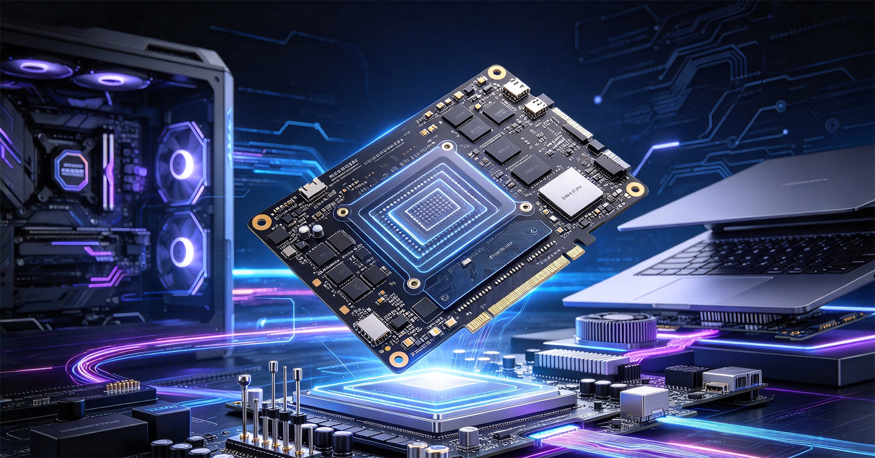
Gaming consoles and high-end laptops are basically high-density computing systems packed into tight mechanical spaces. A modern gaming motherboard may carry a powerful CPU, discrete or integrated GPU, DDR5 memory, high-speed storage, Wi-Fi modules, USB controllers, power management ICs, and advanced cooling sensors. All of these components need clean power, stable signals, and reliable interconnections.
Traditional multilayer PCBs can still work for some applications, but they often struggle when trace density becomes too high. HDI PCBs use Microvias, finer lines and spaces, blind and Buried Vias, and optimized layer stacking to route more signals in less space. This is especially important for:
Honestly, once you start dealing with BGA fan-out and high-speed interfaces, HDI stops being a "nice to have" and becomes a practical necessity.
Modern CPUs, GPUs, and memory controllers use BGAs with hundreds or even thousands of pins. The pad pitch can be very small, which makes traditional through-hole vias inefficient for fan-out. Microvias, typically laser-drilled and much smaller than mechanical vias, allow designers to escape dense BGA areas more cleanly.
In gaming motherboards, microvias help reduce the number of routing layers while maintaining signal quality. They also shorten via stubs, which can improve high-frequency performance. Look, long via stubs are not your friend when you are trying to keep high-speed signals clean.
Blind Vias connect an outer layer to one or more inner layers, while Buried Vias connect only inner layers. Both are commonly used in HDI designs to save space and reduce crosstalk.
For gaming laptops, blind and buried vias allow more efficient routing under high-pin-count components without wasting space on unnecessary through holes. They also help maintain better Impedance Control because the return path can be managed more precisely.
HDI PCBs support finer trace widths and spacing than standard multilayer boards. This is critical when routing high-density digital signals, memory buses, and power distribution networks in a limited area.
Typical HDI designs may use trace widths and spaces around 60 to 75 microns, and advanced processes can go even smaller. Of course, tighter traces mean tighter manufacturing tolerances, so working with a capable supplier matters alot.
High-performance gaming systems are full of fast signals. DDR5 memory, PCIe lanes, display interfaces, and high-speed storage all require careful Impedance Control and noise management. If the PCB layout is not optimized, you can see signal reflection, crosstalk, jitter, or even intermittent failures that are very hard to debug.
HDI structures help because they allow shorter trace lengths, smaller via structures, and better layer planning. But HDI alone does not guarantee good Signal Integrity. You still need solid design practices.
In one laptop motherboard project, moving a PCIe trace away from a switching power inductor reduced measured jitter significantly. The schematic was correct, but the layout created unwanted coupling. That kind of issue is easy to miss until you actually look at the board-level behavior.
Gaming consoles and laptops generate a lot of heat in a small volume. Hdi Boards must handle not only signal routing but also Thermal Management and power delivery. High-current paths for CPU, GPU, and VRM circuits need sufficient copper thickness, proper via count, and low-resistance connections.
At the same time, Thermal Vias are often used to move heat away from hot components into internal copper planes or heatsinks. The challenge is balancing Thermal Performance with signal routing density. If you place too many Thermal Vias near high-speed traces, you may create impedance discontinuities or increase crosstalk risk.
Good practice includes:
Stack-up Design is one of the most important decisions in any HDI project. For gaming motherboards, the stack-up affects impedance, routing density, Thermal Performance, EMI behavior, and manufacturing cost.
A typical HDI stack-up for a high-performance system may include:
One common mistake is choosing a stack-up that looks good on paper but is difficult to manufacture. For example, too many Sequential Lamination steps can increase cost and lead time. A good HDI supplier will review your stack-up and suggest alternatives that keep performance while improving yield.
Gaming hardware is expected to run for long sessions under high load. That means the PCB must be reliable not only at room temperature but also under thermal cycling, vibration, and humidity. Hdi Boards add complexity because microvias and multistep lamination require precise process control.
Key manufacturing considerations include:
For consumer gaming products, manufacturers may also perform drop testing, thermal cycling, and high-temperature storage tests depending on customer requirements. These tests help confirm that microvias and HDI structures can survive real-world use.
HDI PCBs usually cost more than standard multilayer boards because of additional processes such as Laser Drilling, Via Filling, and Sequential Lamination. However, HDI can sometimes reduce total system cost by allowing fewer layers, smaller boards, or simpler assembly.
To manage cost effectively:
Lead time is another factor. HDI boards typically take longer to produce than simple rigid PCBs. If your project is time-sensitive, plan component sourcing and PCB Fabrication in parallel whenever possible.
HDI PCBs allow higher routing density, shorter signal paths, and smaller board sizes. This is especially useful for gaming laptops where space is limited but performance requirements are high.
Not always, but most modern high-performance consoles benefit from Hdi Technology. Complex processors, high-speed memory, and compact mechanical designs make HDI a practical choice for many mainboards.
Via-in-pad places a via directly inside a component pad, usually filled and plated over. It helps with BGA fan-out and thermal performance, but it requires additional manufacturing steps.
Yes. HDI structures are well suited for DDR5 and PCIe 5.0 because they support controlled impedance, shorter vias, and finer routing. Proper Stack-up Design and simulation are still essential.
HDI solutions for high-performance gaming consoles and laptops are not just about making boards smaller. They enable better signal integrity, more efficient power delivery, and higher component density in systems that already operate near their physical limits. For design teams, the key is to choose the right HDI features, validate the stack-up early, and work with a manufacturer that understands high-speed, high-reliability production.
If you are developing a gaming motherboard, console mainboard, or high-performance laptop platform, start your HDI discussion early. Share your impedance targets, BGA requirements, thermal constraints, and testing expectations with your PCB partner. A little upfront planning can save you from costly respins later.
Enabling Compact Designs in True Wireless Stereo (TWS) EarbudsAugust/06/2026
What is High Density Interconnect (HDI) PCB?May/28/2026
Non-Destructive Testing Techniques for Multilayer HDI PCBsSeptember/29/2026
Designing Rugged HDI Boards for Harsh Industrial EnvironmentsJuly/20/2026
Using HDI Technology in Solar Inverters and ConvertersOctober/14/2026
Effective Thermal Management Strategies for High-Density PCBsMay/28/2026
Understanding HDI Terminology: A Glossary for EngineersAugust/03/2026

Key Factors Influencing the Long-Term Reliability of HDI PCBsMay/28/2026