
Modern robotics continues evolving toward smaller footprints, higher performance, and increasingly sophisticated capabilities. Industrial arms perform precise assembly operations while collaborative robots work safely alongside humans. Autonomous mobile robots navigate complex environments while drone systems execute aerial maneuvers. All these systems share a common technological enabler: High Density Interconnect (HDI) printed circuit boards. Hdi Technology provides the Miniaturization, Signal Integrity, and design flexibility that advanced robotics demands, making it essential for next-generation motion control applications.
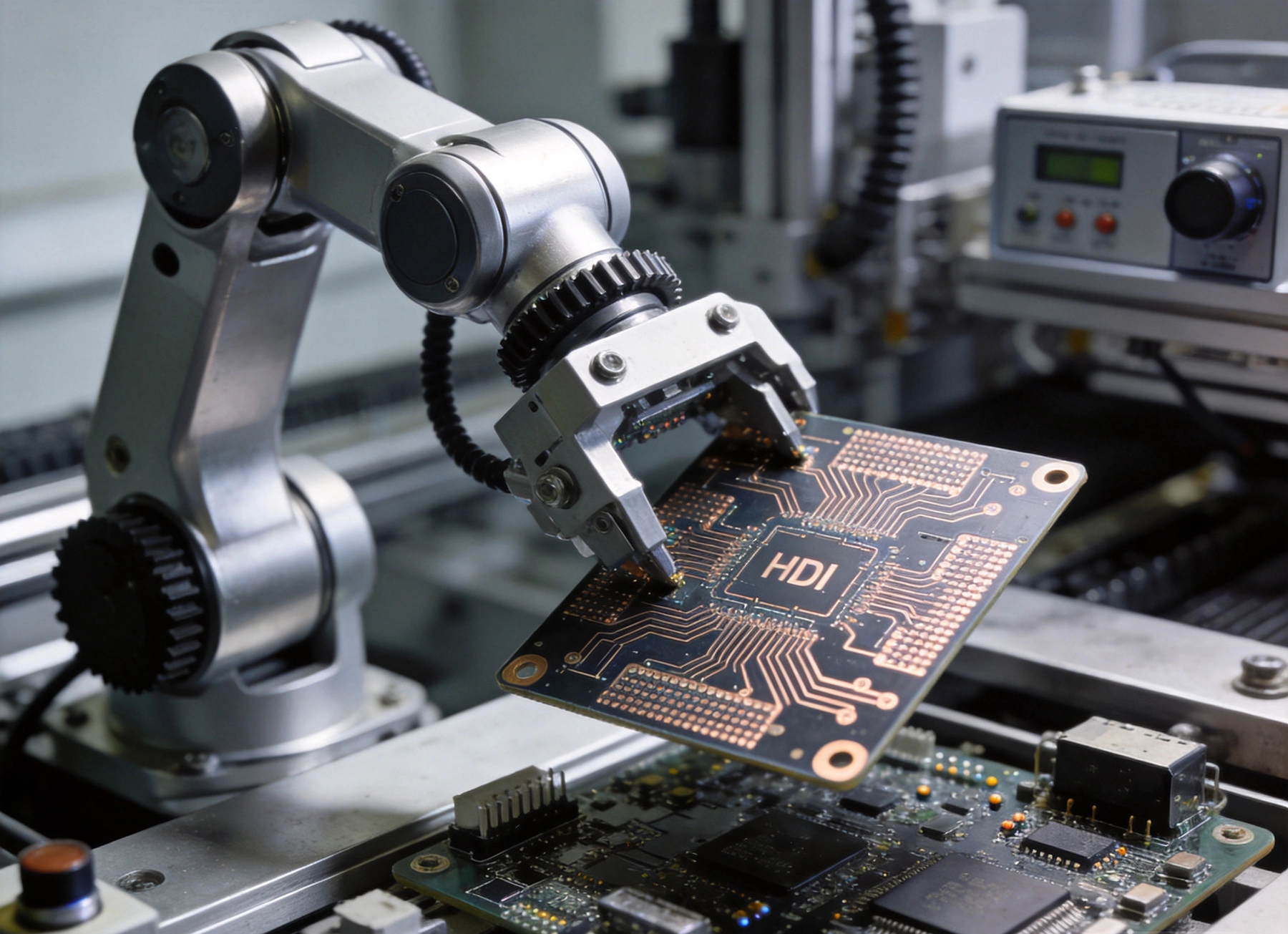
HDI represents a class of PCB construction techniques enabling significantly higher component density than traditional through-hole and multilayer designs. These techniques include Microvias, Blind Vias, Buried Vias, and advanced laminate constructions that maximize routing density while minimizing board area.
Microvia Technology defines HDI capability, with via diameters below 0.15mm compared to standard vias exceeding 0.3mm. These Microvias connect surface layers to inner layers without consuming substantial board area, enabling component placement densities impossible with conventional technologies.
Blind and Buried Vias connect specific layers without penetrating the entire board stack. Blind Vias connect surface layers to inner layers while buried vias connect inner layers without reaching surfaces. This flexibility allows routing optimization and component placement in space-constrained areas.
Any-layer connectivity in advanced HDI constructions allows vias connecting any two layers, maximizing routing flexibility. While this capability adds manufacturing complexity and cost, it enables extremely dense designs impossible with simpler constructions.
Build-up multilayer processes add dielectric and conductor layers sequentially, creating high-density structures without the thermal stress of traditional lamination. These processes suit advanced semiconductor packaging substrates and highly integrated control systems.
Robotics applications push Pcb Design boundaries across multiple dimensions simultaneously. Size constraints, performance requirements, environmental considerations, and reliability expectations all favor HDI approaches.
Collaborative robot compactness requires small form factors allowing deployment in confined spaces and safe operation near humans. HDI enables controller electronics occupying dramatically less volume than equivalent functionality using conventional Pcb Technology.
End-effector electronics including grippers, sensors, and tool changers demand extreme Miniaturization. Wrist-mounted electronics must fit within mechanical envelopes while providing feedback, control, and communication capabilities. HDI makes these Compact Electronics practical.
Sensor integration in robot joints requires electronics capturing encoder feedback, temperature measurements, and torque sensing within mechanical constraints. HDI enables multi-function modules combining these capabilities in single packages.
High-speed communication between distributed controllers demands Signal Integrity exceeding what conventional PCBs easily achieve. HDI's controlled impedance, consistent dielectrics, and minimized discontinuities enable reliable high-speed signaling.
Real-time processing for motion control algorithms requires low-latency signal paths. HDI's shorter routing distances and improved signal quality reduce propagation delays affecting control loop performance.
Power density in compact robot electronics generates heat requiring efficient distribution and dissipation. HDI's layer count flexibility allows optimized power plane distribution and thermal via placement.
Complex routing for multi-axis control systems benefits from HDI's routing density and via flexibility. Signal routing between processors, motor drivers, and sensors can be optimized without board-area constraints limiting placement options.
Component integration through packages like BGA and QFN becomes practical when HDI enables fan-out routing from high-pin-count devices. Without HDI techniques, these packages would be unroutable at reasonable board sizes.
Modular architectures using card-edge connectors benefit from HDI's ability to route signals efficiently to connector areas. Standard pitch connectors combined with fine-pitch internal routing maximizes I/O density.
Motion control encompasses diverse systems from simple servo drives to complex multi-axis controllers. Each application leverages HDI capabilities differently.
Power stage PCBs in servo drives benefit from HDI's ability to combine Power Electronics with control circuits in compact packages. Gate drivers, current sensing, and control processors share board space efficiently through HDI construction.
Gate driver isolation requirements for high-side switching demand precise control circuitry placement. HDI enables isolation barriers without consuming excessive board area or creating routing constraints.
Current sensing circuits require careful analog layout to achieve accurate feedback. HDI's consistent dielectric properties and controlled impedance support precision analog design.
Processor cards executing motion planning algorithms benefit from HDI enabling high-pin-count processor packages and extensive memory interfaces. Modern processors with hundreds of ball grid array connections become practical through HDI fan-out techniques.
Communication interfaces including EtherCAT, PROFINET, and Ethernet POWERLINK require high-speed physical layers. HDI provides the signal integrity these protocols demand while maintaining compact form factors.
Feedback interfaces for encoders, resolvers, and torque sensors populate motion controllers with diverse signal types. HDI accommodates differential pairs, single-ended signals, and isolated interfaces without layout compromises.
Integrated joint electronics combining motor drive, position feedback, and communication in single modules exemplify HDI miniaturization benefits. These modules must fit within joint envelopes defined by mechanical design requirements.
Thermal Management in joint modules requires careful power dissipation within constrained volumes. HDI enables Thermal Vias and heat spreading structures that conventional PCBs cannot efficiently implement.
Reliability under vibration demands robust constructions addressing mechanical stress. HDI's reduced drilling and more uniform construction can improve vibration performance compared to thick-board alternatives.
Implementing HDI in robotics applications requires balancing competing requirements and understanding manufacturing constraints.
Layer count optimization depends on circuit complexity, routing requirements, and budget constraints. Robotics applications typically use 4-8 layers with Microvia Technology rather than expensive any-layer constructions.
Dielectric thickness control affects impedance consistency and manufacturing yield. HDI constructions require tighter thickness tolerances than standard multilayer boards, impacting material selection and fabrication approaches.
Via-in-pad technology places vias directly beneath component pads, maximizing routing density. This technique requires careful design rules and solder mask coverage to prevent solder wicking into vias during assembly.
Standard HDI materials including FR-4 and high-Tg alternatives provide cost-effective solutions for many robotics applications. These materials handle standard HDI processing without special accommodations.
Low-loss dielectrics benefit high-speed signal paths in communication and processing circuits. While adding cost, these materials improve signal integrity at elevated frequencies.
Flexible and rigid-flex constructions enable electronics conforming to mechanical envelopes in robot designs. HDI techniques apply to polyimide substrates enabling flexible interconnects between rigid sections.
Minimum line and space resolutions vary by manufacturer capability and construction type. Typical HDI capabilities include 75μm lines and spaces, with advanced capabilities reaching 50μm or tighter.
Via aspect ratios limit Microvia depth-to-diameter ratios. Manufacturing constraints affect minimum Microvia sizes and layer-to-layer connections possible in single drilling operations.
Registration accuracy between layers becomes critical as feature sizes shrink. HDI manufacturers maintain tighter registration tolerances through advanced imaging and processing controls.
Hdi Manufacturing adds cost compared to conventional PCBs, but overall system economics often favor HDI despite higher per-board expenses.
Size reduction value provides the primary economic justification when board area reduction offsets HDI cost premiums. Smaller enclosures, reduced housing costs, and simplified mechanical designs contribute to total value.
Performance improvements in signal integrity, latency, and power distribution may justify HDI costs when system performance directly impacts product value or customer requirements.
Integration benefits from combining functions on single boards reduce connector costs, simplify assemblies, and improve reliability. These savings may offset HDI premiums for complex systems.
Layer count minimization reduces HDI costs by using microvia technology for routing efficiency rather than adding layers. Start with minimum layers meeting routing requirements before adding layers for space.
Standard construction selection avoiding advanced Any-layer Hdi reduces costs while maintaining most miniaturization benefits. Sequential Lamination with controlled depth drilling often satisfies robotics requirements at lower cost.
Panel efficiency optimization through array design, fiducial placement, and panel utilization improves yields and reduces per-board costs. Manufacturer consultation during layout can identify optimization opportunities.
Comparing HDI against alternatives helps determine appropriate technology selection for specific applications.
Routing density comparison shows HDI achieving 2-4x density improvement through microvia efficiency and finer line/space capabilities. For robotics applications requiring component-dense designs, this density advantage enables smaller boards.
Cost comparison typically shows 20-50% HDI premiums over equivalent standard multilayer boards. This premium decreases for more complex standard designs where HDI enables layer count reduction.
Reliability comparison generally favors HDI for vibration applications due to reduced drill sizes and more uniform construction. Thermal cycling performance depends on specific constructions and materials.
Application suitability differs significantly between technologies. Flexible circuits suit dynamic interconnects while HDI suits dense static circuits. Many robotics applications benefit from combinations of both technologies.
Rigid-flex constructions combining HDI rigid sections with flexible interconnects provide both density and flexibility. These hybrid constructions suit applications needing dense electronics with mechanical movement.
Hdi Technology continues advancing alongside robotics capabilities, enabling new application possibilities.
Embedded component technology places passive components within PCB layers, further reducing surface area requirements. Capacitors and resistors embedded in power distribution layers improve electrical performance while saving space.
Substrate-like PCB constructions blur boundaries between IC substrates and Pcb Technology. These ultra-high-density constructions enable levels of integration previously limited to semiconductor packaging.
Thermal via optimization continues improving heat extraction from dense HDI designs. Advanced thermal via constructions including filled and cap-plated vias provide efficient heat paths.
Metal core HDI combinations bring Thermal Management benefits of metal substrates together with HDI routing density. These constructions suit high-power-density robotics applications.
Low-temperature co-fired ceramic (LTCC) alternatives provide ceramic-like electrical properties with PCB-compatible processing. These materials suit high-frequency applications within robotics.
Bio-based laminates emerging for environmental sustainability may offer electrical properties suitable for robotics applications. While early in development, these materials may become viable alternatives.
Manufacturing HDI PCBs for robotics requires partners with appropriate capabilities and quality systems.
Microvia manufacturing capabilities including Laser Drilling, alignment systems, and plating processes determine minimum feature sizes and via aspect ratios achievable. Verify capabilities against specific design requirements.
Quality systems including IPC standards compliance, statistical process control, and incoming inspection ensure consistent manufacturing. Request documentation of capability studies and process controls.
Test and inspection capabilities for HDI require advanced approaches due to via accessibility limitations. Automated Optical Inspection, X-ray Inspection, and electrical test coverage should be evaluated.
DFM review capabilities help optimize designs for manufacturing before fabrication. Early engagement with manufacturers identifies potential issues before they become expensive problems.
Material expertise guides selection of appropriate dielectrics, prepregs, and surface finishes for specific application requirements. Manufacturers with robotics experience understand relevant trade-offs.
Prototype support enables design validation before committing to production volumes. Look for partners offering prototype services using production-equivalent processes.
HDI technology has become essential for advanced robotics and motion control systems, enabling the miniaturization, performance, and integration that modern applications demand. From collaborative robots to multi-axis controllers to integrated joint modules, HDI PCBs provide the foundation for compact, high-performance motion control electronics.
Understanding HDI fundamentals, design considerations, and cost trade-offs enables informed technology selection. While HDI adds manufacturing complexity and cost, overall system benefits often justify the investment through size reduction, improved performance, and enhanced reliability.
Partner selection requires evaluating microvia capabilities, quality systems, and engineering support. Manufacturers experienced with robotics applications understand the specific requirements and can guide optimization for manufacturing efficiency.
As robotics continues advancing toward greater capability and deployment diversity, HDI technology will remain foundational. Emerging trends including embedded components, thermal integration, and new materials will expand possibilities while maintaining HDI's essential role in enabling next-generation motion control systems.
Typical HDI capabilities include 75μm lines and spaces with 150μm microvias. Advanced manufacturers achieve 50μm lines and spaces with 100μm microvias. Ultra-advanced constructions reach finer dimensions but at significantly higher cost and with limited manufacturing sources.
HDI improves signal integrity through consistent dielectric properties, controlled impedance capability, and reduced discontinuities. Shorter routing paths reduce parasitic inductance while microvia structures minimize stub effects that degrade high-speed signals.
No, HDI provides benefits primarily for applications requiring high component density, small board sizes, or high-speed signals. Simpler robotics applications with standard components and relaxed space constraints may achieve cost savings using conventional PCB technology.
Robotics applications typically require thermal cycling, vibration testing, and humidity exposure testing. IPC standards define test methods and acceptance criteria. Specific requirements depend on application environment and reliability expectations.
Yes, rigid-flex HDI constructions combining dense rigid sections with flexible interconnects can significantly reduce wiring complexity in robotics applications. Flexible sections replace cables and connectors while rigid sections provide dense electronics mounting.
HDI Solutions for In-Vehicle Infotainment (IVI) and ClustersAugust/07/2026
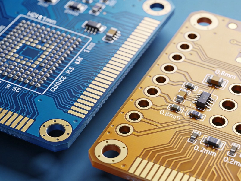
Understanding the Core Differences Between HDI and Traditional PCBsJuly/02/2026

The Role of HDI in Avionics and Flight Control SystemsAugust/13/2026
Meeting AEC-Q100 Reliability Standards for Automotive HDISeptember/14/2026
Designing Automotive HDI Boards for Vibration and Shock ResistanceJuly/17/2026

How HDI Technology Supports Advanced Driver Assistance Systems (ADAS)June/25/2026
Key Factors Influencing the Long-Term Reliability of HDI PCBsMay/28/2026
What is the Lead Time for Manufacturing Custom HDI Boards?October/12/2026