Open Nav

The aerospace industry stands at the forefront of electronic innovation, demanding reliability, performance, and Miniaturization that push the boundaries of what printed circuit board technology can achieve. Flight control systems, navigation computers, communication equipment, and sensor arrays all require electronics that can operate flawlessly in extreme conditions while meeting stringent weight and space constraints. High-density Interconnect technology has emerged as an essential enabler for meeting these demanding requirements, providing the foundation upon which modern avionics systems are built.
Avionics electronics must satisfy requirements that far exceed those of commercial electronics. Altitude changes create thermal cycling challenges. Vibration from engines and aerodynamic forces stress components and interconnects. Electromagnetic interference from multiple systems demands careful design for Signal Integrity. Regulatory requirements from agencies including the FAA and EASA mandate extensive qualification processes that verify performance under these harsh conditions. Hdi Technology provides the reliability foundation that makes qualification possible.
The evolution from conventional through-hole technology to surface mount and finally to HDI has driven dramatic improvements in avionics capability. Today's flight computers process millions of calculations per second, integrating data from dozens of sensors to provide pilots with actionable information and enabling automated flight functions. These advances would be impossible without the density, performance, and reliability that HDI provides. Understanding the role of HDI in avionics illuminates the connection between Pcb Technology and the aircraft systems upon which modern aviation depends.

Modern avionics systems encompass a wide range of functions that demand increasingly sophisticated electronics. Flight management computers integrate navigation, performance optimization, and communication into unified systems. Primary flight displays present attitude, altitude, airspeed, and navigation information with unprecedented clarity. Autopilot systems process sensor inputs and adjust control surfaces to maintain stable flight. Each of these systems relies on PCBs that must deliver computing power, reliability, and real-time responsiveness under all flight conditions.
The physical environment within aircraft creates Pcb Design challenges that differ dramatically from ground-based applications. Temperature ranges span from frigid conditions at cruise altitude to heating from electronic dissipation. Pressure variations affect dielectric properties and can stress component packages. Vibration frequencies from engines and aerodynamics can fatigue solder joints and loosen connectors. Humidity, when it occurs during flight operations, creates moisture challenges. Hdi Technology addresses these challenges through enhanced materials, superior interconnects, and design practices developed specifically for aerospace applications.
Weight and space constraints in aircraft create pressure to minimize electronics size while maximizing functionality. Every kilogram of electronics reduces payload capacity or fuel efficiency. Every cubic centimeter of avionics bay space trades against other systems or passenger amenities. HDI technology enables dramatic size reduction through increased routing density, smaller component packages, and more efficient layer utilization. These density improvements translate directly into weight savings and space optimization that benefit the entire aircraft.
Aerospace Electronics must satisfy extensive regulatory requirements before installation in certificated aircraft. DO-254 for airborne electronic hardware and DO-178C for software define the development processes and verification activities necessary to demonstrate airworthiness. These standards impose documentation requirements, process controls, and validation activities that exceed those for commercial electronics by orders of magnitude. PCB suppliers serving aerospace must implement quality management systems that satisfy these requirements.
Material selection for aerospace avionics PCBs follows more restrictive guidance than commercial applications. Flammability requirements under FAR 25.853 mandate materials that resist ignition and limit flame spread. Outgassing requirements for space and vacuum applications prevent contamination of optical systems. Thermal cycling capability must be demonstrated across the expected service temperature range. HDI materials for aerospace applications are selected and tested to demonstrate compliance with these specialized requirements.
Traceability requirements in aerospace extend from raw material through finished assemblies. Every component, every process step, and every test result must be documented and retained throughout the service life of the aircraft plus additional years for investigation purposes. HDI suppliers serving aerospace must implement traceability systems that capture this information and make it available when regulators, customers, or investigation teams require access.
HDI technology delivers multiple benefits that address the specific requirements of avionics and flight control systems. The most apparent benefit is Miniaturization, achieved through finer line geometries, smaller vias, and higher layer counts. However, HDI provides additional advantages that may be equally important for aerospace applications: improved reliability, enhanced Signal Integrity, and better Thermal Management. These combined benefits make HDI the technology of choice for virtually all advanced avionics systems.
The miniaturization enabled by HDI directly addresses weight and space constraints in aircraft. Component packages continue shrinking, with chip-scale packages and wafer-level chip scale packages requiring HDI routing to fan out from tiny ball arrays to board traces. Microvia Technology enables routing density impossible with conventional processes, allowing more functionality in smaller volumes. These density improvements compound throughout the aircraft, reducing the weight and space burden of avionics systems.
Reliability improvements from HDI stem from multiple design and manufacturing factors. Microvias eliminate the barrel discontinuities that affect conventional through-holes, reducing stress concentrations that can cause failure under thermal cycling. The Sequential Lamination used for complex HDI structures enables controlled expansion characteristics that reduce thermal stress on components. Higher routing density often enables simpler routing with fewer layers and vias, reducing the number of potential failure points.
Microvia Reliability in aerospace applications has been demonstrated through extensive testing and field experience. The small dimensions of Microvias, while presenting manufacturing challenges, provide reliability advantages over larger through-holes. The absence of long barrel structures eliminates resonance issues that can affect through-hole performance under vibration. Stress concentrations that cause fatigue failures in larger structures are distributed across the smaller HDI geometries.
Thermal cycling reliability testing demonstrates HDI capability for aerospace temperature ranges. Qualification testing subjects boards to hundreds of temperature cycles spanning the expected service range, with thermal soak periods that accelerate potential failure mechanisms. Microvia structures consistently demonstrate superior thermal cycling performance compared to through-hole alternatives, validating their use in applications where temperature excursions are frequent and severe.
Vibration testing verifies HDI performance under the mechanical stresses encountered during flight. High-frequency vibration from turbine engines and low-frequency vibration from aerodynamic loads create different failure modes that testing must address. HDI structures, with their distributed architecture and minimized stress concentrations, demonstrate excellent vibration tolerance. Combined with appropriate component mounting practices, HDI assemblies meet the most demanding vibration requirements.
Flight control systems represent the most demanding avionics application, directly affecting aircraft safety and controllability. Fly-by-wire systems replace mechanical linkages with electronic signals, requiring computing systems that can process pilot inputs and sensor feedback in real-time to command hydraulic or electric actuators. These systems demand computing performance, deterministic response, and fault tolerance that push Pcb Technology to its limits.
The electronics architecture for fly-by-wire systems typically employs multiple redundant computers that cross-check each other to detect and isolate failures. This redundancy provides safety assurance even when individual components fail. However, redundancy multiplies the electronics content in the aircraft, increasing the importance of miniaturization through HDI technology. Without HDI, the weight and space required for redundant flight control computers would be prohibitive.
Sensor integration in flight control systems creates demanding PCB requirements. Angle of attack sensors, load factor sensors, position sensors, and rate sensors all feed data to flight control computers. Signal conditioning electronics must process these varied inputs with precision that supports the accuracy requirements of flight control algorithms. HDI enables the mixed-signal design density necessary to locate signal conditioning close to sensors while maintaining the digital processing density for control law computation.
Autopilot systems have evolved from simple stability augmentation to sophisticated flight management that controls aircraft throughout all phases of flight. Modern autopilots integrate with flight management systems that optimize trajectories for fuel efficiency, emissions reduction, and noise abatement while maintaining safety margins. These integrations require computing performance that demands the density HDI provides.
Display systems present flight information with graphics quality that rivals consumer electronics, driven by requirements for clarity and situational awareness. High-resolution displays with video processing, graphics acceleration, and multiple video inputs create PCB density requirements that conventional technology cannot satisfy. HDI enables the routing density, controlled impedance, and signal integrity that high-resolution display processing demands.
Communication and navigation systems integrate with flight management to support RNAV, RNP, and satellite-based navigation approaches. These systems must process signals from multiple sources including GPS, inertial reference systems, VOR receivers, and datalink systems. Signal routing for these diverse RF and digital signals requires the layer utilization and shielding that HDI provides, while maintaining the isolation necessary to prevent interference between systems.
Designing HDI PCBs for aerospace applications requires attention to requirements that extend beyond typical commercial practice. Design for manufacturing must account for the specialized processes aerospace HDI suppliers use. Design for testability must ensure that hidden structures and components can be verified. Design for reliability must address the specific failure mechanisms that affect Aerospace Electronics. These considerations shape design practices throughout the development process.
Layer stack design for aerospace HDI must address signal integrity, power delivery, and Thermal Management simultaneously. Multiple ground planes provide shielding and low-impedance return paths. Power planes distribute current while contributing to decoupling capacitance. Signal routing layers provide the routing resources for high-density components. The stack must be optimized for the specific application requirements while maintaining manufacturability and reliability.
Via strategy selection depends on the specific requirements of each design. Through-hole vias provide the mechanical robustness required for some applications despite their size disadvantages. Blind Vias connect surface layers to internal layers without penetrating the entire board. Buried Vias connect internal layers without surfacing. Stacked and staggered Microvia configurations enable the routing density that HDI provides. The designer must select the via strategy that meets application requirements while remaining within manufacturing capability.
Material selection for aerospace HDI begins with the base laminate system. Polyimide materials provide superior thermal stability for high-temperature applications and excellent mechanical properties for vibration environments. BT-Epoxy offers a balance of Thermal Performance and processing ease. High-speed materials with controlled dielectric constants address signal integrity requirements for high-frequency applications. The selection must balance electrical, thermal, and mechanical requirements against cost and availability.
Prepreg and core selection determines the dielectric properties and thermal characteristics of the layer stack. Material thicknesses must satisfy Impedance Control requirements while providing adequate breakdown voltage for high-voltage applications. The coefficient of thermal expansion must be compatible with components and other materials to minimize thermal stress. Material lot traceability for aerospace applications ensures that properties remain consistent across production.
Metal finishing selection affects both reliability and manufacturability. ENIG provides excellent flatness for fine-pitch component mounting and good solderability. Electroplated gold over nickel provides superior contact resistance for edge connectors. Lead-free finishes must be evaluated for their thermal cycling performance compared to traditional tin-lead. The finish must be compatible with the components being mounted and the assembly processes being used.
Aerospace Hdi Manufacturing demands capabilities and quality systems that exceed typical commercial PCB production. The combination of fine geometries, complex structures, and stringent reliability requirements creates manufacturing challenges that require specialized equipment, skilled personnel, and robust process controls. Understanding these requirements helps system designers appreciate the complexity and cost of aerospace electronics production.
Laser Drilling for microvia formation requires specialized equipment and precise process control. The laser parameters must be optimized for the specific material system, with pulse energy, repetition rate, and focus position controlled to achieve consistent via geometry. Multiple laser passes may be required for deeper structures, with each pass adding to cycle time and potential variation. The Laser Drilling process must be validated and monitored to maintain the consistency that aerospace quality requires.
Sequential Lamination for complex HDI structures requires careful process control to prevent defects. Each lamination cycle subjects previously processed layers to elevated temperature and pressure that could damage components or degrade structures. Process parameters including temperature, pressure, and dwell time must be optimized for the specific stack configuration. Process validation must demonstrate that the cumulative effects of multiple lamination cycles do not compromise reliability.
Aerospace HDI inspection employs techniques beyond those used for commercial boards. X-ray Inspection verifies internal structures including microvia quality, layer alignment, and internal voids. Cross-section analysis provides definitive evaluation of structural quality at specific locations. These destructive and semi-destructive tests are performed on process qualification samples and periodically during production to verify ongoing capability.
Electrical testing for aerospace HDI must verify continuity, isolation, and impedance characteristics across the entire board. High-potential testing confirms that dielectric materials can withstand the voltage stresses they may encounter in service. Test equipment must have sufficient resolution to detect the small impedance variations that can affect signal integrity. Test coverage must address all nets including those that are not directly accessible.
Acceptance testing for aerospace HDI follows detailed test procedures that document every step and verify every result. Flying probe testing or bed-of-nails testing provides complete net verification. Boundary Scan testing addresses complex ICs with limited physical access. Functional test at the board or subsystem level verifies that the assembled electronics perform as specified. All test results must be documented and retained as part of the traceability record.
Aerospace Hdi Reliability must be demonstrated through qualification testing that verifies performance under expected service conditions. Qualification testing follows established standards and protocols that define test conditions, sample sizes, and acceptance criteria. Successful qualification provides the confidence necessary for regulatory approval and customer acceptance of avionics systems.
Thermal cycling testing exposes HDI assemblies to repeated temperature excursions that simulate flight conditions. Chambers cycle temperature between specified limits while monitoring for opens, shorts, or parameter drift. Test severity is defined by the temperature range, ramp rates, and dwell times that simulate worst-case service conditions. Microvia integrity is verified through these tests, with failure analysis performed on any rejects to identify root causes.
Vibration testing simulates the mechanical environment of flight including launch vibrations, cruise vibrations from engines and aerodynamics, and landing loads. Fixtures must transmit vibration to the test article without adding resonant frequencies that could mask or amplify responses. Test levels and durations are defined by the specific aircraft and flight envelope. HDI assemblies must survive these tests without damage that could affect function or safety.
When qualification or production testing reveals failures, systematic failure analysis determines root causes and corrective actions. The analysis must proceed systematically from symptom to root cause, verifying hypotheses through testing and examination. For HDI assemblies, failure modes may involve microvia structures, laminate materials, plating quality, or component interfaces. Identifying the specific failure mode guides corrective action selection.
Corrective action for HDI failures may involve design changes, process changes, or both. Design changes might include increased annular rings, modified routing to reduce stress, or different material selection. Process changes might include modified drilling parameters, improved cleaning procedures, or adjusted lamination cycles. All corrective actions must be validated to confirm their effectiveness and must not introduce new failure modes.
Lessons learned from failure analysis inform future designs and processes. Documented failure modes and corrective actions create knowledge bases that prevent recurrence in subsequent projects. This continuous learning improves reliability and reduces qualification costs over time. Organizations that systematically capture and apply these lessons develop expertise that differentiates them in the demanding aerospace market.
Aerospace electronics continues evolving toward greater integration, higher performance, and enhanced capabilities. These advances drive continued evolution of HDI technology and the design practices that apply it. Understanding emerging trends helps system architects plan future systems and helps PCB specialists prepare the capabilities that will be required.
Miniaturization trends point toward even finer geometries and more complex layer structures. Embedded passives eliminate discrete components, reducing assembly complexity and improving performance. Embedded actives place bare die directly in the PCB, achieving densities impossible with surface mount technology. These advanced approaches require Hdi Manufacturing capabilities that extend beyond current practice.
Wide-bandgap semiconductors including silicon carbide and gallium nitride enable Power Electronics with improved efficiency and Thermal Performance. These devices operate at higher temperatures and voltages than traditional silicon, requiring Pcb Materials and designs that accommodate these stresses. HDI technology provides the thermal management capabilities that wide-bandgap devices demand.
More-electric aircraft architectures replace hydraulic and pneumatic systems with electrical alternatives, increasing the role of Power Electronics in aircraft systems. High-power motor drives, power conversion systems, and battery management systems require PCBs with capabilities beyond traditional avionics. These applications demand HDI with heavy copper, advanced thermal management, and reliability demonstrated for high-power stress.
Power electronics miniaturization through HDI enables installation of electrical systems in locations that could not accommodate conventional approaches. Distributed power architectures place power conversion close to loads, reducing distribution losses while simplifying installation. HDI enables the density necessary for these distributed architectures while maintaining the thermal and reliability characteristics that power electronics require.
Wide-bandgap devices in aircraft power systems drive material and design evolution. The higher operating temperatures of silicon carbide and gallium nitride devices challenge traditional Pcb Materials and assembly processes. New material systems optimized for high-temperature operation extend the capability of HDI technology to serve these demanding applications.
Q: What HDI structures are used in flight control systems?
A: Flight control systems typically employ sequential lamination with multiple build-up layers, Stacked Microvias for routing density, and through-hole constructions for mechanical robustness where needed. The specific structure depends on component density, routing requirements, and reliability targets. Most advanced flight control systems use multiple HDI build-up layers on both sides of core substrates.
Q: How is Hdi Reliability verified for aerospace applications?
A: Aerospace HDI reliability is verified through qualification testing per DO-160 for environmental conditions and ARP 5996 for HDI-specific requirements. Testing includes thermal cycling, vibration, humidity, and thermal shock. Test samples are evaluated at defined intervals and must demonstrate acceptable performance without failure. Statistical analysis of results confirms that reliability targets are met.
Q: What are the cost implications of aerospace HDI versus commercial alternatives?
A: Aerospace HDI typically costs significantly more than commercial HDI due to lower volumes, more stringent process controls, extensive documentation, and specialized materials. However, the cost premium is justified by the reliability requirements, regulatory compliance, and extended service life that aerospace applications demand. Total cost of ownership, including failure costs and support requirements, often favors the higher initial investment.
Q: How does HDI affect the development timeline for avionics systems?
A: HDI implementation typically extends development timelines due to additional design iterations for manufacturing optimization, longer qualification cycles, and more extensive documentation. However, the density and performance benefits of HDI often enable simpler system architectures that reduce overall development complexity. Early engagement with HDI suppliers helps optimize timelines.
Q: What emerging HDI technologies will affect future avionics?
A: Emerging technologies include embedded active and passive components, photonic integration, advanced substrates for high-power applications, and manufacturing techniques that reduce cost while maintaining aerospace quality. These technologies will enable further miniaturization, improved performance, and new capabilities for avionics systems.
HDI technology has become indispensable for avionics and flight control systems, providing the foundation upon which modern aircraft electronics are built. The miniaturization, reliability, and performance benefits of HDI address the demanding requirements of aerospace applications in ways that conventional technology cannot match. As aircraft systems continue evolving toward greater integration and capability, the importance of HDI will only increase.
The challenges of aerospace HDI implementation—from specialized materials through demanding manufacturing processes to extensive qualification requirements—create barriers that limit the supplier base to those with proven capabilities. This concentration of capability in experienced suppliers provides assurance that aerospace electronics meet the stringent requirements that flight safety demands. System developers benefit from this expertise while accepting the lead times and costs that aerospace quality requires.
Future developments in HDI technology will enable avionics systems with capabilities beyond current imagination. From embedded intelligence to photonic interconnects, the evolution of HDI will parallel the evolution of aircraft systems themselves. Organizations that invest in understanding and applying HDI technology position themselves to participate in the continuing advancement of aviation electronics that makes flight safer, more efficient, and more capable.

HDI Solutions for In-Vehicle Infotainment (IVI) and ClustersAugust/07/2026
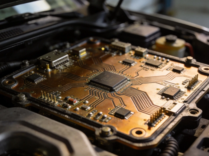
Meeting AEC-Q100 Reliability Standards for Automotive HDISeptember/14/2026

How HDI Technology Supports Advanced Driver Assistance Systems (ADAS)June/25/2026
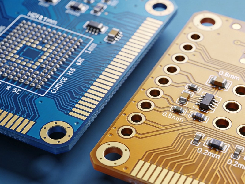
Understanding the Core Differences Between HDI and Traditional PCBsJuly/02/2026
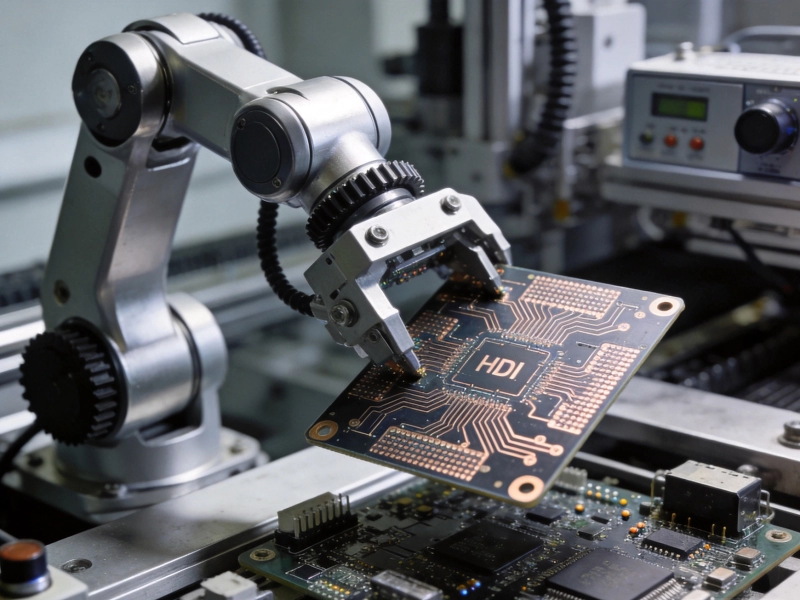
The Role of HDI in Robotics and Motion Control SystemsAugust/10/2026
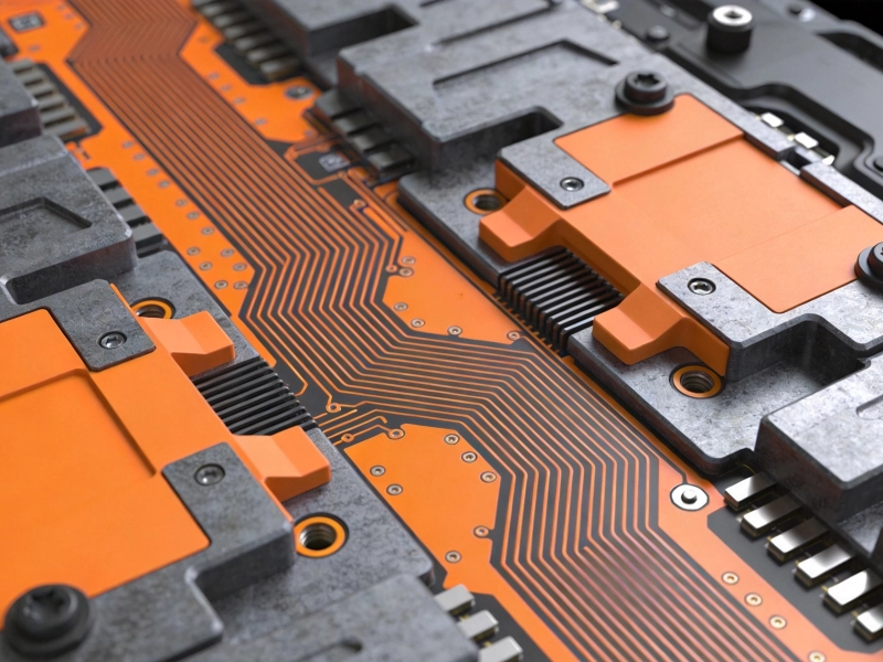
Designing Automotive HDI Boards for Vibration and Shock ResistanceJuly/17/2026
Signal Integrity Challenges in 5G mmWave HDI DesignsAugust/08/2026
The Importance of Electrical Testing for Microvia ReliabilityJuly/09/2026