Open Nav

High-density Interconnect (HDI) Pcb Design is constantly pushing the limits of how thin, dense, and high-performance printed boards can be. For years, the bottleneck in advancing HDI capability was the Dielectric Material between copper layers: traditional prepreg and core materials rely on glass fiber cloth as a reinforcing skeleton, which sets a practical lower limit on dielectric layer thickness, introduces signal distortion from glass weave effects, and complicates Microvia formation in ultra-thin layers. Resin Coated Copper (RCC) solves all these problems by ditching the glass fiber entirely, creating a material system that is tailor-made for the Sequential Lamination build-up processes that define modern Hdi Manufacturing.
RCC is not just another Dielectric Material. It is a fundamental reimagining of how the insulating layer and conductive copper layer are produced together, eliminating the lamination interface between prepreg and copper foil in the build-up layer. This single change opens up new possibilities for board thickness reduction, Signal Integrity improvement, and manufacturing yield enhancement that would be impossible with traditional material stacks. This article breaks down what RCC actually is, why it has become a standard material in advanced HDI production, how it fits into the Sequential Lamination workflow, and the practical considerations designers and manufacturers need to account for when using it.
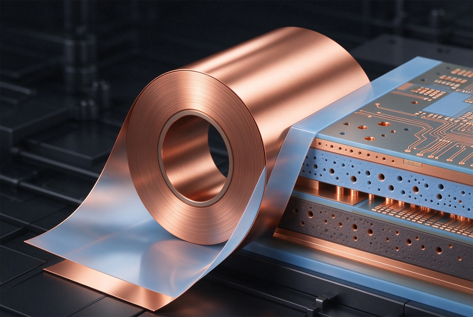
As the name suggests, Resin Coated Copper is a two-layer composite material: a thin layer of electrolytic copper foil with a uniform coating of thermoset insulating resin applied directly to one side. The resin is typically an epoxy-based formulation, sometimes blended with BT (Bismaleimide Triazine), PPE (Polyphenylene Ether), or PI (Polyimide) resins for high-temperature or high-frequency applications. Unlike traditional prepreg, there is no glass fiber cloth embedded in the resin layer — the cured resin itself has sufficient structural integrity to form the entire dielectric layer between copper conductors.
The thickness of the resin layer is tightly controlled during the coating process, ranging from as little as 15 μm up to around 100 μm depending on the application. The copper foil thickness typically ranges from 12 μm to 35 μm for most HDI use cases, though thicker foils are available for power delivery layers in high-current designs. This combination of ultra-thin resin and thin copper allows build-up layers as thin as 30 μm total, which is impossible to achieve with traditional prepreg and copper foil combinations due to the minimum thickness of the glass fiber cloth.
The manufacturing process for RCC is highly controlled to ensure consistent resin thickness, uniform resin distribution, and reliable adhesion between the resin and copper foil. The resin is applied to the copper in a semi-cured (B-stage) state, similar to prepreg, so it flows and cures fully during the lamination process. This semi-cured state allows the resin to fill in micro-roughness on the underlying copper layer during lamination, creating an excellent bond between layers without voids.
The most immediately obvious advantage of RCC is its ability to produce dielectric layers far thinner than traditional glass-reinforced prepreg. Glass fiber cloth used in standard prepreg has a minimum thickness of around 50 μm for even the thinnest grades, which sets a floor on how thin a build-up layer can be. RCC eliminates that floor entirely, enabling dielectric layers as thin as 15 μm. This is critical for the most advanced HDI designs, particularly those using any-layer interconnection, where multiple thin build-up layers are stacked sequentially to maximize routing density without increasing the overall board thickness.
For a smartphone main board using 6 to 8 build-up layers, switching from traditional prepreg to 25 μm RCC reduces the total board thickness by more than 0.2 mm compared to using 50 μm prepreg. That may sound like a small difference, but in a device where the total board thickness is under 1 mm, it is the difference between fitting additional components or leaving out features to meet industrial design constraints.
Glass fiber prepreg introduces Signal Integrity problems that become increasingly severe as signal frequencies climb above 5 GHz. The woven glass fiber structure creates regions of higher dielectric constant (the glass fiber itself, Dk ~6) and lower dielectric constant (the resin filling the gaps between fibers, Dk ~3.5). When a high-speed signal trace runs parallel to a glass fiber bundle, it experiences a different effective Dk than a trace running perpendicular to the bundle, leading to differential skew between signals in a differential pair that causes bit errors at high data rates.
RCC has no glass fiber structure at all, so the dielectric constant is perfectly uniform across the entire layer area. This eliminates glass weave skew entirely, and also reduces Insertion Loss because the resin used in RCC typically has a lower loss tangent (Df) than glass-reinforced prepreg. For high-speed serial links running at 10 Gbps and above, this signal integrity improvement alone justifies the RCC material cost premium.
This advantage has become increasingly important for 5G, 6G, and High-speed Computing applications. 1.6T optical module PCBs and high-speed server backplanes rely on RCC to achieve the consistent dielectric performance required to maintain signal integrity across hundreds of high-speed differential pairs, without the complex trace routing angles and length matching schemes needed to compensate for glass weave effects in traditional material stacks.
Microvias are the foundation of HDI design, and RCC makes Microvia Drilling and plating significantly more reliable than with traditional prepreg-copper stacks. In a traditional HDI build-up, the Microvia is drilled through the copper foil and the underlying prepreg layer. The interface between the copper and prepreg creates a risk of delamination during drilling or plating, and the glass fiber in the prepreg can cause drill wander, resin smear, and incomplete hole cleaning during desmear.
With RCC, the copper and the underlying resin layer are bonded during the material manufacturing process, not during PCB lamination. This eliminates the delamination risk at the copper-resin interface, and the pure resin layer drills more cleanly than glass-reinforced prepreg. Laser Drilling of Microvias in RCC produces smoother hole walls, less resin smear, and more consistent hole diameters across the panel, which improves plating uniformity and reduces the risk of microvia opens or reliability failures under thermal cycling.
Because the resin adheres so well to the copper foil, the via sidewall has better plating adhesion too. Microvias formed in RCC have consistently higher thermal cycling reliability than those formed in traditional prepreg stacks, especially when stacked vertically across multiple build-up layers. This reliability advantage is critical for automotive and industrial Hdi Boards that must survive thousands of thermal cycles over a multi-year service life.
The thinner dielectric layers enabled by RCC allow designers to use narrower trace widths and spacing while maintaining the same characteristic impedance for controlled impedance traces. A 50-ohm single-ended trace on a 25 μm RCC dielectric can be as narrow as 40 μm, compared to around 75 μm on a 50 μm traditional prepreg layer. This narrower trace width increases routing density by nearly 50% on the same layer area, which means a design that would have required four signal layers with traditional prepreg can often be routed in three layers with RCC, reducing total layer count and overall board cost.
Even when layer count stays the same, the higher routing density allows more complex designs to fit on a smaller board footprint, reducing material cost and enabling smaller product form factors. For high-volume consumer electronics, this density advantage directly translates to lower per-unit cost, as more boards can be panelized on a single production panel.
In traditional HDI sequential lamination, each build-up cycle requires aligning and laminating a prepreg layer and a copper foil layer separately to the underlying core. This adds alignment steps and increases the risk of misregistration between layers, as well as the risk of trapped air or voids between the prepreg and copper. With RCC, the copper and resin are supplied as a single unified sheet, so each Build-up Lamination cycle only requires aligning one material sheet instead of two. This simplifies the process, reduces cycle time, and improves layer-to-Layer Registration accuracy, which directly increases manufacturing yield for high-density designs.
The unified material also reduces the number of material interfaces in the stackup, which reduces the risk of delamination during thermal cycling. Delamination between prepreg and copper layers is a common failure mode in thick Hdi Boards exposed to extreme temperature swings, and eliminating those interfaces directly improves long-term reliability.
RCC is designed to integrate seamlessly into existing sequential lamination Hdi Manufacturing processes, with only minor adjustments to process parameters.
The process starts with a finished core board that has already been drilled, plated, and etched. The first RCC layer is laminated to the core under heat and pressure, which cures the semi-cured resin fully and bonds it to the underlying copper traces. After lamination, the outer copper layer of the RCC is etched to form the first build-up layer signal traces and pads. Microvias are then laser-drilled through the RCC layer to connect to the underlying core pads, desmeared to remove resin residue, plated, and filled if required.
Each additional build-up layer follows the same sequence: laminate RCC to the previous layer, etch the outer copper, drill and plate microvias, repeat as needed. This sequence is identical to the traditional sequential lamination process, except that the prepreg and copper foil steps are combined into a single RCC lamination step.
For stacked microvia designs, where a microvia on one build-up layer is placed directly on top of a microvia on the layer below, RCC's uniform resin layer and clean drilling characteristics ensure reliable interconnection between vias. The consistent resin thickness also means the via aspect ratio stays consistent across all build-up layers, which improves plating uniformity and reduces the risk of voids in the via barrel.
While RCC offers significant advantages, it is not a drop-in replacement for prepreg in all designs, and it introduces its own set of process requirements that manufacturers must account for.
The semi-cured resin coating on RCC is sensitive to ambient temperature, humidity, and UV light. If RCC is stored at too high a temperature, the resin can advance in cure degree prematurely, which reduces its flow during lamination and leads to poor bonding between layers. If exposed to high humidity, the resin absorbs moisture, which causes voids and delamination during lamination. Most RCC materials have a shelf life of 3 to 6 months when stored in controlled temperature and humidity conditions, and they must be brought to room temperature in sealed packaging before use to avoid condensation.
These handling requirements add operational complexity compared to traditional prepreg, which generally has a longer shelf life and more forgiving storage conditions. Manufacturers who are new to RCC typically need to update their material storage and handling procedures to avoid material degradation before use.
The resin in RCC has different flow characteristics than standard prepreg, so the lamination pressure, temperature profile, and dwell time must be adjusted to ensure complete resin flow, void-free lamination, and full cure. If the lamination temperature is too low, the resin does not flow enough to fill the underlying copper topography, leading to voids and poor adhesion. If the temperature is too high, the resin flows too much and gets squeezed out from between layers, leading to inconsistent dielectric thickness.
Most RCC suppliers provide recommended lamination profiles specific to their material, but manufacturers typically need to run qualification lamination runs to optimize the profile for their specific equipment and stackup design. This qualification process adds time and cost to the first production run of a new RCC-based design.
While RCC drills more cleanly than glass-reinforced prepreg, the pure resin layer requires different desmear parameters after Laser Drilling. The desmear process uses chemical etchants to remove resin residue from the via sidewalls before plating, and the etch rate on pure RCC resin is different than on glass-reinforced prepreg. If the desmear time is too short, residual resin remains on the via sidewall and prevents good plating adhesion. If the etch time is too long, the etchant attacks the resin layer excessively and can undercut the copper pad at the top of the via, leading to reliability issues.
For mechanical drilling of through-holes that pass through RCC layers, the lack of glass fiber actually reduces drill wear, so drill life is longer than with traditional prepreg stacks. This reduces tooling cost over the long run, though the difference is minimal for designs with only a few build-up layers.
RCC is more expensive per unit area than traditional prepreg-copper foil combinations, typically by 20% to 40% depending on the resin formulation and thickness. This cost premium is justified in high-density, high-speed designs where the material advantages translate to lower layer count, higher yield, or better signal performance. For low-cost, low-density HDI designs, however, the cost premium may be difficult to justify unless the design specifically requires the ultra-thin dielectric capability that only RCC can provide.
It's important to note that the direct material cost is not the only economic consideration. The reduced lamination cycle time, higher yield, and reduced layer count that RCC enables can offset the material cost premium in many high-volume designs. For example, reducing a board from six layers to four layers with RCC can reduce total manufacturing cost even if the material cost per layer is higher, because fewer lamination cycles are required.
RCC has become the standard material for advanced HDI designs in several high-growth electronics segments:
Smartphone and Wearable Electronics benefit from RCC's ultra-thin dielectric capability, which allows manufacturers to pack more functionality into thinner, lighter devices. Flagship smartphones have used RCC in their main boards for over a decade, and the material is now standard in smartwatches, wireless earbuds, and other compact Wearables.
High-speed communications infrastructure — 5G base stations, 1.6T optical modules, high-speed server backplanes — relies on RCC's uniform dielectric constant and low loss tangent to maintain signal integrity at multi-gigabit data rates. The elimination of glass weave skew is particularly critical for these applications, where even a few picoseconds of differential skew can cause a link to fail bit error rate requirements.
Automotive Adas (Advanced Driver Assistance Systems) and In-vehicle Infotainment modules use RCC for its combination of high routing density and high thermal cycling reliability. The automotive environment subjects electronics to extreme temperature swings, vibration, and humidity, and RCC's excellent via reliability and reduced delamination risk directly improve long-term product life.
Aerospace and defense electronics benefit from RCC's light weight, high reliability, and radiation resistance. The absence of glass fiber reduces the amount of secondary radiation generated when high-energy particles pass through the board, which improves performance in space and high-altitude applications.
Resin Coated Copper is more than just an incremental improvement to existing HDI materials. It is a foundational technology that has enabled the last decade of advances in electronics Miniaturization and high-speed communication. By eliminating the glass fiber skeleton that limited traditional dielectric materials, RCC opened the door to thinner, denser, more reliable HDI boards with signal performance that would have been impossible to achieve with older material systems.
While RCC has limitations in handling requirements and cost, its advantages in density, signal integrity, and manufacturing yield make it the material of choice for any advanced HDI design where performance, Miniaturization, or reliability is a priority. As signal speeds continue to climb and product form factors continue to shrink, RCC will only become more essential to the future of Pcb Manufacturing.
Contact us to discuss your requirements.
The Challenge of Plating and Filling Microvias in HDI ProductionJuly/26/2026
Critical Quality Checkpoints in the HDI Production LineJuly/13/2026
Overcoming Common Manufacturing Defects in High-Density InterconnectsSeptember/21/2026
Precision in HDI FabricationJune/04/2026
Understanding Sequential Lamination in Multi-Step HDI BoardsJuly/03/2026
How Manufacturers Achieve High Precision Alignment in 10+ Layer HDI BoardsAugust/15/2026

What is the Lead Time for Manufacturing Custom HDI Boards?October/12/2026
The Role of Laser Drilling in Advancing HDI PCB CapabilitiesOctober/23/2026