Open Nav

Every time you pull out your smartphone, scroll through a fitness tracker, or rely on Medical Electronics to monitor your health, you're interacting with technology that was simply impossible to manufacture a couple of decades ago. The devices that fit in your pocket today pack more computing power and connectivity than room-sized computers from the 1970s, and the circuit boards inside them are engineering marvels that push the boundaries of what's physically possible. A big part of how we got here involves Laser Drilling—a manufacturing technique that has quietly enabled the density and performance of modern electronics.
Mechanical drilling simply can't achieve the hole sizes and precision that today's HDI (High-density Interconnect) boards require. When you need via diameters measured in tens of microns rather than hundreds, you need a different approach. Laser Drilling fills that gap, and understanding how it works helps explain why modern electronics look and perform the way they do.
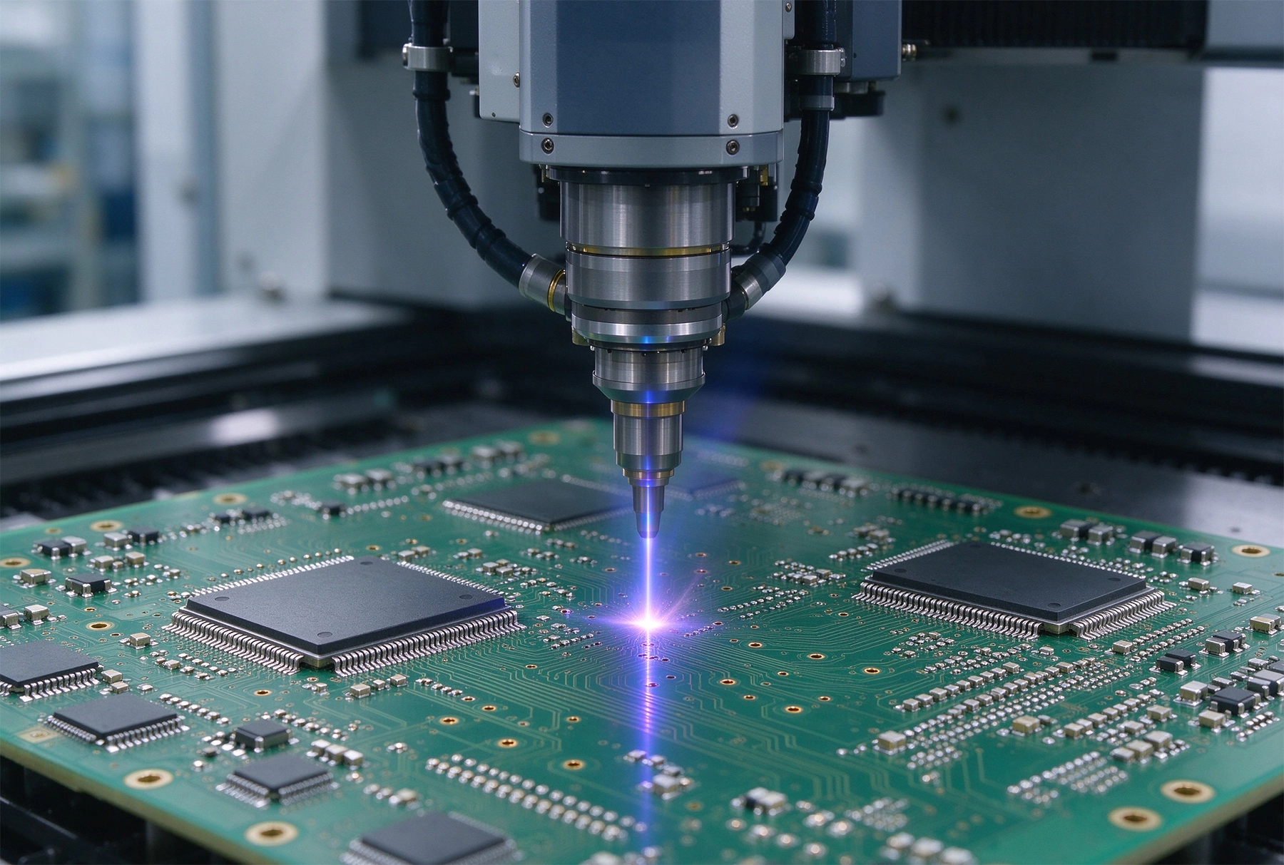
High-density Interconnect boards are designed to maximize functionality in minimum space. They achieve this through several techniques: finer trace widths and spacing, more routing layers, and most importantly, Microvias that connect layers with minimal space consumption. The Microvia is the defining feature of HDI, and it demands manufacturing capabilities that mechanical drilling simply cannot provide.
Traditional plated through holes (PTH) in standard PCBs might be 0.3mm to 0.8mm in diameter. These holes pass through the entire board thickness and consume significant board area. In an HDI context, you might need vias that are 0.1mm or smaller, and these holes might only pass through one or two layers rather than the full stack. The combination of smaller diameter and selective depth makes laser drilling not just preferable but essential.
Hdi Boards typically use multiple types of vias in a hierarchy that serves both electrical and manufacturing requirements. Through vias connect outer layers to inner layers and are often still mechanical. Blind Vias connect an outer layer to one or more inner layers without penetrating the full board. Buried Vias connect only inner layers and are hidden from the outer surfaces.
Laser drilling is particularly valuable for blind and buried Microvias because it can drill to precise depths without affecting layers below the target. This selective drilling capability is what makes complex HDI stackups possible. You can have multiple Microvia layers, each connecting different combinations of signal and plane layers, all packed into a board thickness that would be impossible with through-hole technology.
The laser drilling process sounds simple in principle—you use a laser beam to remove material where you want a hole. In practice, it's a sophisticated process that requires precise control over energy delivery, beam positioning, and material interaction. Different laser types and drilling strategies serve different purposes in Pcb Manufacturing.
Two main types of lasers are used in PCB drilling: CO2 lasers and UV (solid-state) lasers. Each has different characteristics that make it suitable for different applications.
CO2 lasers operate at infrared wavelengths around 10.6 micrometers. They are well absorbed by the organic materials in PCB substrates—primarily the epoxy and glass fiber that make up FR-4 and similar materials. CO2 lasers can drill through resin efficiently but have difficulty cutting through copper. For this reason, Co2 Laser Drilling is typically used for sequential build-up processes where the target layer is exposed copper anyway.
UV lasers operate at wavelengths around 355nm (for Nd:YAG UV) or shorter. The shorter wavelength means higher photon energy, which allows UV lasers to ablate almost any material including copper. UV laser drilling can cut through copper, resin, and glass fiber indiscriminately, making it more versatile but also more complex to control. The process creates a heat-affected zone that must be managed carefully to avoid damage to surrounding materials.
Laser drilling removes material through a process called ablation. The laser energy is absorbed by the material, which heats rapidly and vaporizes or is ejected from the surface. For PCB substrates, this process is relatively straightforward—the organic materials absorb laser energy well and vaporize cleanly. For copper, the process is more complex because copper reflects much of the incident laser energy at certain wavelengths.
Modern laser drilling systems use multiple passes with decreasing spot sizes to create via walls with the proper taper and cleanliness. The first pass removes most of the material, while subsequent passes clean up the walls and floor of the via. This staged approach produces better quality than trying to drill the full depth in a single pass.
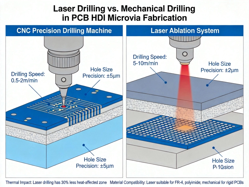
Mechanical drilling has served Pcb Manufacturing well for decades, and it remains the right choice for many applications. Through-hole vias of conventional sizes are drilled economically with mechanical equipment. But for HDI microvias, mechanical drilling reaches fundamental physical limits.
The smallest practical mechanical drill bit is limited by its strength. A drill bit that is too small relative to its length will break before it penetrates the board. For very small holes, even if you could drill them mechanically, the holes would be too small to plate reliably. The aspect ratio—depth divided by diameter—becomes extreme, and plating solution can't flow through the narrow hole to deposit copper uniformly on the walls.
Mechanical drilling accuracy is limited by drill bit deflection, spindle runout, and board handling. As hole sizes decrease, these error sources become more significant relative to the hole size itself. A 0.05mm positional error in a 0.3mm hole is a small fraction of the hole diameter. The same error in a 0.1mm hole is half the hole diameter—completely unacceptable.
Laser drilling achieves much better positional accuracy because there is no physical contact between the tool and the workpiece. The laser beam is positioned with precision motion stages and optical systems, achieving accuracy measured in microns rather than the tens of microns typical of mechanical drilling.
For mass production, laser drilling systems use a step-and-repeat approach where the board is positioned under the laser, a field of vias is drilled, and then the board moves to the next position. Modern systems can drill thousands of vias per second, making the process economically viable for high-volume production despite the per-via time being longer than mechanical drilling for larger holes.
The economics of laser drilling depend heavily on via count and board size. For boards with many small vias, laser drilling is the only viable option. For boards with few large vias, mechanical drilling remains faster and cheaper. The manufacturing engineer must choose the right approach based on the specific board requirements.
Laser drilled microvias require different Quality Control approaches than mechanically drilled holes. The small size makes manual inspection impossible, and the different failure modes require specialized testing.
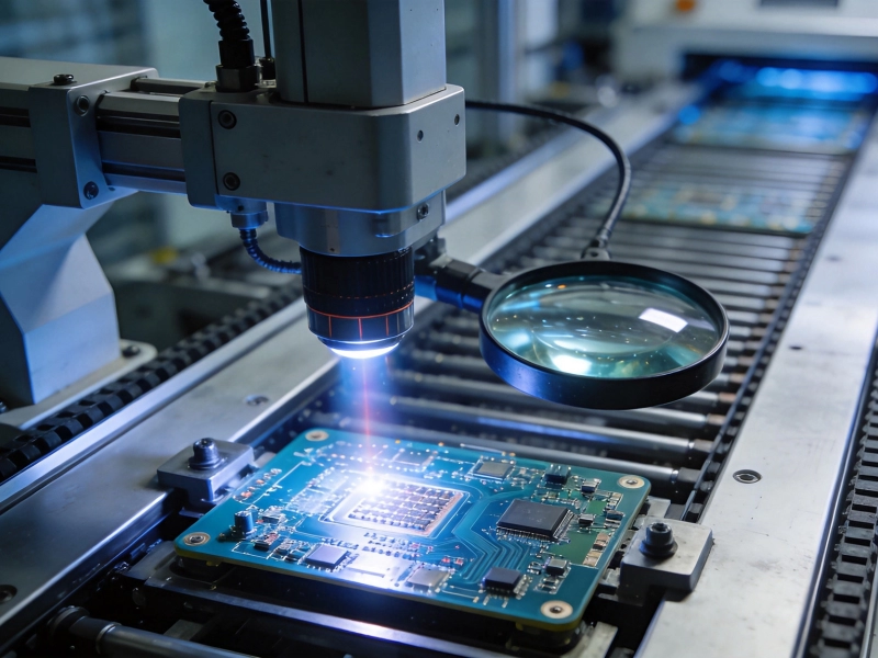
Laser drilled vias should have straight walls with clean, well-defined corners at the top and bottom. The bottom of the via should be flat and free of debris. Any resin smear, copper nodules, or contamination on the via walls will affect plating quality and electrical reliability. Automated Optical Inspection systems examine via geometry at high magnification to detect defects that would be invisible to the naked eye.
X-ray Inspection is used to verify via quality after plating. Because microvias are so small, cross-sectional analysis is impractical for production monitoring. X-ray imaging allows inspection of the via barrel and plating without destroying the sample.
Microvias have different reliability characteristics than larger through holes. Their small size means less plating thickness per unit area and different thermal expansion behavior. Microvias in Hdi Boards are often the most thermally stressed features in the stackup, and reliability testing must specifically evaluate microvia performance.
Thermal cycling tests, often to military or automotive standards depending on the application, verify that microvias can survive the temperature excursions expected in service. Failure analysis on boards that fail thermal testing helps identify whether the failure is in the via itself or in the surrounding laminate.
The capabilities and limitations of laser drilling directly affect how HDI stackups are designed. Understanding these constraints helps you work with your PCB manufacturer to achieve the best possible result.
Many HDI boards use a sequential build-up (SBU) process where layers are added one at a time rather than being drilled through the full stack. In this approach, a base substrate gets processed, then dielectric is applied, then copper is deposited, then the next layer's pattern is defined. Laser drilling creates vias through the newly added dielectric to connect to the underlying copper pattern.
The SBU approach allows extraordinary routing density because each layer pair can have its own dedicated microvia connection. However, it requires precise process control at each step and careful design to ensure that the accumulated tolerances don't create misregistration problems.
The most advanced HDI boards use any-layer interconnection, where any layer can connect to any other layer through microvias. This maximum flexibility comes at a cost—Any-layer Hdi boards require more build-up steps and more laser drilling than simpler stackups. The manufacturing complexity translates to higher cost and longer lead times.
For many applications, a more conservative HDI approach with fewer any-layer connections provides most of the density benefit at significantly lower cost. The right balance depends on your specific routing requirements and volume expectations.
Laser drilling technology continues to advance, enabling even finer features and more complex HDI designs. Several development directions are worth watching.
Ultrafast lasers that generate pulses in the picosecond or femtosecond range offer advantages for Microvia Drilling. The extremely short pulse duration means less thermal energy is transferred to surrounding material, reducing the heat-affected zone and improving via quality. These lasers are becoming more practical for production as the technology matures and costs decline.
Advanced laser drilling systems now incorporate real-time monitoring of via quality during the drilling process. Rather than drilling all vias and then inspecting afterward, these systems detect problems immediately and adjust parameters to maintain consistent quality. This inline approach reduces the impact of variation in material properties or other process factors.
Modern Hdi Manufacturing combines laser drilling with other processes in sophisticated sequences. Laser Via formation is followed by desmear to clean the via walls, then by electroless copper deposition, then by electrolytic plating to build up the final copper thickness. Each step must be optimized for the specific combination of materials and via geometry, and the process flow continues to evolve as manufacturers seek better results.
Laser drilling adds cost to PCB manufacturing compared to purely mechanical processes. The equipment is expensive, the process is slower per via, and the specialized expertise required commands a premium. Understanding where these costs come from helps you evaluate whether the investment is worthwhile for your application.
Laser drilling systems represent significant capital investment. UV lasers suitable for drilling copper are particularly expensive due to the sophisticated optics and motion control required. The facilities housing these systems need vibration isolation, clean rooms, and precise environmental control—all of which add to the overhead that gets allocated to boards processed on the equipment.
Even with the fastest modern systems, laser drilling takes longer per via than mechanical drilling. For high-volume production of boards with many microvias, this processing time adds significant cost. The economics improve as laser technology advances and faster systems become available, but laser drilling will likely always carry a cost premium over mechanical drilling for comparable hole sizes.
The cost premium for laser drilling is justified when the alternative—using larger holes or a less dense board—would require a larger board, more layers, or a more expensive assembly approach. The total system cost often decreases when you optimize at the board level rather than trying to minimize Pcb Manufacturing Cost in isolation.
If your design requires HDI microvias, choosing the right manufacturing partner and communicating clearly about your requirements are essential for success.
Not all PCB manufacturers have laser drilling capability, and among those that do, capability levels vary significantly. Ask potential partners about their laser equipment, minimum via sizes, aspect ratio limits, and any volume restrictions. Request samples of their work to evaluate quality directly rather than relying on specifications alone.
Your manufacturer should provide design rules specific to their laser drilling capabilities. These rules define minimum via sizes, spacing requirements, stackup constraints, and other parameters that affect your layout. Following these rules closely improves your chances of getting manufacturable boards on the first spin.
Good manufacturers also provide DFM feedback that identifies features in your design that might cause problems. Take this feedback seriously—manufacturers have seen thousands of designs and understand what works in production better than most designers do.
Laser drilling is the enabling technology for Hdi Pcb Manufacturing. Without it, the via densities required for modern smartphones, Wearables, and other Compact Electronics would simply be impossible to achieve. Understanding the capabilities and limitations of laser drilling helps you make better design decisions and communicate more effectively with your manufacturing partners.
The choice between CO2 and UV laser drilling depends on your specific stackup and via requirements. CO2 lasers work well for resin-only drilling in sequential build-up processes. UV lasers provide the versatility to drill through copper when needed but require more sophisticated process control.
Quality Control for laser-drilled microvias requires different approaches than traditional Pcb Inspection. Automated optical and X-ray Inspection systems are essential for verifying the quality of microvias that are too small to inspect manually.
The cost premium for laser drilling is often justified by the system-level benefits of Hdi Technology. A slightly more expensive HDI board that fits in a smaller enclosure with fewer layers may be the most cost-effective overall solution for your product.
Contact us to discuss your Hdi Pcb requirements and how laser drilling capabilities can support your design objectives.
What is the Lead Time for Manufacturing Custom HDI Boards?October/12/2026
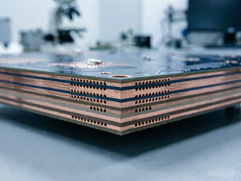
Understanding Sequential Lamination in Multi-Step HDI BoardsJuly/03/2026
Overcoming Common Manufacturing Defects in High-Density InterconnectsSeptember/21/2026
The Challenge of Plating and Filling Microvias in HDI ProductionJuly/26/2026
Precision in HDI FabricationJune/04/2026
Critical Quality Checkpoints in the HDI Production LineJuly/13/2026
How Manufacturers Achieve High Precision Alignment in 10+ Layer HDI BoardsAugust/15/2026
Meeting AEC-Q100 Reliability Standards for Automotive HDISeptember/14/2026