Medical devices play by different rules than consumer electronics. A pacemaker PCB failure doesnt cause a reboot—it can cause a life-threatening event. A glucose monitor that leaches contaminants through the skin violates every regulatory standard that exists. The PCB inside a surgical instrument must survive sterilization temperatures that would delaminate a standard FR-4 board in a single cycle. When you add HDI (High Density Interconnect) technology to the mix—which is increasingly necessary for miniaturized implantable and wearable medical devices—the design challenge compounds. HDI brings Blind Vias, Microvias, and Sequential Lamination that introduce new reliability risk factors precisely where medical applications can least tolerate them. This article addresses the specific requirements, material choices, and design strategies for creating biocompatible and safe Hdi Boards that meet the stringent demands of medical use.

Why Medical PCBs Demand a Different Design Approach
The difference between a medical PCB and a standard industrial PCB is not just tighter tolerances—it is a fundamentally different design philosophy rooted in risk management. Medical device development follows ISO 14971 risk management processes, and the Pcb Design decisions must be traceable to that risk framework.
Key factors that set medical PCBs apart:
- Patient contact implications: Boards in implantable devices are in direct contact with body tissue. Boards in wearable monitors contact skin. Even boards in hospital equipment may expose patients to outgassing chemicals or conductive leakage currents.
- Regulatory scrutiny: FDA, EU MDR, and other regulators review PCB material choices and design decisions as part of device submission. You need documentation showing that every material is biocompatible or adequately isolated from patient contact.
- Sterilization survival: Autoclave (steam at 134°C), ethylene oxide gas, hydrogen peroxide plasma, and gamma radiation all stress Pcb Materials differently. A board that survives one cycle may degrade over 50+ reprocessing cycles.
- Long service life with zero maintenance: An implantable PCB may need to operate flawlessly for 10–15 years inside the body with no possibility of repair. There is no scheduled maintenance window.
These requirements shape every downstream decision—from laminate selection to via reliability qualification to surface finish choice.
Biocompatibility: More Than Just Material Certification
Biocompatibility for medical PCBs is governed by ISO 10993, which defines a series of tests evaluating biological responses to materials. For PCB substrates and surface finishes, the relevant test categories include cytotoxicity (cell death), sensitization (allergic response), and irritation. Passing ISO 10993 testing is necessary but not sufficient—you also need to ensure that the complete assembly process does not introduce biocompatibility hazards.
Substrate Materials for Biocompatible HDI Boards
Standard FR-4 uses a brominated epoxy resin system for flame retardancy. Brominated compounds can raise cytotoxicity concerns, particularly for implantable applications where leaching into surrounding tissue is possible. Alternative substrate options for biocompliant medical Hdi Boards:
- Non-brominated FR-4 (halogen-free): Uses phosphorus-based or nitrogen-based flame retardants instead of bromine. Meets IEC 61249-2-21 halogen-free requirements. Better biocompatibility profile while maintaining process compatibility with standard HDI fabrication. This is the most practical choice for most medical HDI boards.
- Polyimide: Excellent thermal stability (Tg > 250°C), survives autoclave sterilization, and has a well-established biocompatibility record in implantable electronics. The tradeoff is higher cost and more difficult HDI processing—polyimide is hygroscopic and requires careful moisture control during lamination and plating.
- LCP (Liquid Crystal Polymer): Increasingly used in miniaturized medical devices, LCP offers extremely low moisture absorption (0.04%), excellent chemical resistance, and stable electrical properties. Its thin-film form factor is well-suited for flexible and rigid-flex medical HDI constructions. LCP requires specialized via formation (Laser Drilling) but produces reliable Microvias with good plating adhesion.
- Ceramic (HTCC/LTCC): For the most demanding implantable applications—neurostimulators, cochlear implants—ceramic substrates offer hermetic sealing capability and complete biocompatibility. However, ceramic HDI processing is fundamentally different from organic PCB processing, with much higher cost and limited design flexibility.
Surface Finishes and Patient Safety
The PCB surface finish is critical for biocompatibility because it is the outermost layer that contacts the environment—and potentially the patient. Common surface finishes ranked by biocompatibility concern:
- ENIG (Electroless Nickel / Immersion Gold): The nickel layer contains phosphorus and can cause sensitization reactions in nickel-allergic patients. For implantable devices, ENIG is generally avoided on any surface that could contact tissue. For non-contact medical equipment, ENIG is acceptable and provides excellent wire bondability and solderability.
- ENEPIG (Electroless Nickel / Electroless Palladium / Immersion Gold): The palladium layer between nickel and gold provides a diffusion barrier that prevents nickel ion migration. Much better biocompatibility profile than ENIG for patient-proximate applications. Increasingly specified for wearable and skin-contact medical PCBs.
- Hard gold over nickel: Used for connector contacts that undergo repeated insertion cycles. The gold layer must be thick enough (30+ μin) to prevent nickel exposure through porosity. Acceptable for external connectors but not for implantable surfaces.
- Immersion silver: Good solderability and biocompatibility for non-implantable applications. Silver has antimicrobial properties which can be beneficial in hospital environments. Vulnerable to tarnish and creep corrosion that can affect long-term reliability.
- Immersion tin: Biocompatible and lead-free. Used where wire bonding or press-fit connections are needed. Susceptible to whisker growth, which is a reliability concern for long-life medical devices.
For implantable HDI boards, the safest approach is a thin pure gold surface (electroplated, not immersion) over a barrier layer that prevents copper migration. The gold must be thick enough to be non-porous (typically 1–2 μm) but thin enough to avoid gold embrittlement of solder joints (keep below 3 μm for soldered connections).
HDI Reliability for Medical Applications: The Microvia Challenge
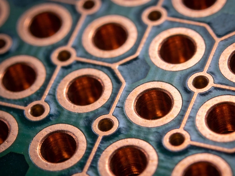
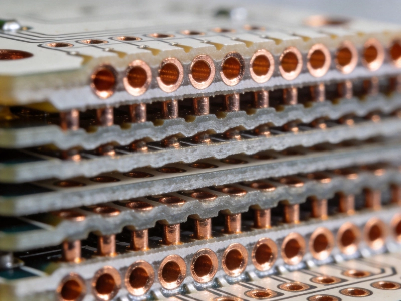
Hdi Technology enables the Miniaturization that medical devices demand—blind microvias at 4-mil diameter allow BGA fan-out that would be impossible with through-hole vias. But microvias are the weakest structural element in an HDI board, and their failure modes are precisely the ones that medical applications cannot tolerate.
Microvia Failure Mechanisms
The primary failure mode for microvias is separation at the interface between the via Copper Plating and the capture pad (target pad) below. This interface is created during Sequential Lamination—its not a drilled and plated through-hole with continuous barrel copper. The separation is driven by:
- Cte Mismatch stress: Copper (17 ppm/°C) and FR-4 (14–18 ppm/°C in-plane, 50–70 ppm/°C z-axis) expand at different rates. Every thermal cycle stresses the Microvia neck where it meets the capture pad.
- Moisture absorption and outgassing: If moisture is trapped in the dielectric beneath the Microvia during lamination, it can vaporize during reflow soldering, creating pressure that delaminates the via from the capture pad—sometimes called popcorning.
- Plating quality variation: The aspect ratio of a microvia (depth divided by diameter) affects plating uniformity. Aspect ratios above 0.8:1 become difficult to plate consistently, particularly at the via bottom where solution agitation is limited.
Design Rules for Medical-Grade Microvias
Given the failure risk, medical HDI microvias require more conservative design rules than consumer HDI:
- Maximum aspect ratio 0.5:1: For a 4-mil diameter microvia, limit depth to 2 mils. This means single-layer microvias only—no skip-layer (staggered) connections through two dielectric layers in a single via, even though the technology supports it.
- Minimum capture pad size: 12-mil capture pad for a 4-mil microvia (3:1 ratio). Larger pads provide more adhesive area and reduce stress concentration at the via-to-pad interface.
- Via fill requirement: All microvias under component pads must be copper-filled and planarized. Epoxy-only fill is not acceptable for medical applications because epoxy does not provide the structural reinforcement that copper fill offers against via collapse under thermal cycling.
- Staggered, not stacked: Never use Stacked Microvias (one via directly on top of another) in medical HDI boards. Stacked vias concentrate all interfacial stress at a single point and have significantly lower thermal cycling reliability. Staggered vias (offset on adjacent layers) distribute stress and are much more robust.
Qualification Requirements
IPC-6012 Class 3 is the baseline requirement for medical PCBs, but for implantable devices, even Class 3 may not be sufficient. Additional qualification steps:
- IST (Interconnect Stress Test): Accelerates Microvia Fatigue failure by resistive heating. A medical HDI board should pass 1000+ IST cycles at 150°C peak temperature. This is far more aggressive than the standard 300-cycle qualification.
- Thermal cycling per Ipc-9701: Minimum 2000 cycles at -40°C/+125°C for implantable devices, with no detectable resistance increase in microvia chains. This testing takes months to complete but provides the confidence level that medical risk management demands.
- Moisture resistance per IPC-540: Verify that moisture absorption during storage and handling does not create outgassing risk during lead-free reflow. Medical HDI boards should meet MSL level 1 (unlimited floor life) or level 2 (1 year) at minimum.
Cleanliness and Contamination Control
Medical device cleanliness requirements go far beyond standard electronics cleanliness. IEC 60601-1 and ISO 10993 both address the risk of chemical contamination from the PCB reaching the patient. For HDI boards in particular, contamination trapped in microvias and between closely spaced traces can be extremely difficult to remove.
Process Cleanliness Standards
The key cleanliness metrics for medical HDI boards:
- Surface ionic contamination: Measured by ion chromatography or ROSE testing. Medical boards typically require < 0.1 μg NaCl equivalent per cm², which is 5× stricter than standard IPC cleanliness requirements.
- Residual flux: Any flux residue in via holes, under components, or between fine-pitch leads is a potential leachable contaminant. No-clean flux processes are generally preferred for medical boards because they minimize residue, but the no-clean flux must itself be evaluated for biocompatibility if the board will be in patient contact.
- Particulate contamination: HDI fabrication generates fine debris from Laser Drilling and desmear processes. Particles trapped in microvias can create conductive paths or obstruct Via Filling. Medical HDI boards require enhanced cleaning protocols—multiple cleaning cycles with both solvent spray and ultrasonic agitation.
- Outgassing: All materials in the board assembly must be evaluated for volatile organic compound (VOC) outgassing, particularly for enclosed implantable devices where released chemicals cannot escape. NASA outgassing standards (ASTM E595, < 1.0% TML, < 0.1% CVCM) provide a useful baseline for medical applications as well.
Cleanroom Assembly Considerations
For implantable and invasive medical devices, PCB assembly should occur in a controlled cleanroom environment (ISO Class 7 or better). This controls both particulate contamination and biological contamination—bacteria, endotoxins, and other biological residues on the board surface could cause infection or inflammatory response if the device is implanted.
Cleanroom assembly requirements include:
- Personnel in cleanroom garments with proper gowning procedures
- Controlled material entry with wipe-down and transfer protocols
- Soldering and handling equipment rated for cleanroom use (no particle-generating fans, belt drives, or compressed air sources)
- Post-assembly visual inspection under magnification with particle counting
- Endotoxin testing (LAL test) for devices classified as invasive
Electrical Safety: Leakage Current and Isolation
IEC 60601-1 defines strict limits for patient leakage current and patient auxiliary current in medical electrical equipment. The Pcb Design directly affects whether these limits can be met.
Creepage and Clearance for Medical Isolation
Medical devices often require 2 MOPP (Means of Patient Protection) or 2 MOOP (Means of Operator Protection) isolation between patient-connected circuits and mains voltage. This translates to specific creepage and clearance distances on the PCB:
- Creepage (surface distance): For 250V working voltage at 2 MOPP, IEC 60601-1 requires 4mm creepage on the PCB surface (pollution degree 2, material group IIIa). This is significantly larger than the 0.4mm clearance that standard industrial designs might use at the same voltage.
- Clearance (air distance): 2 MOPP at 250V requires 1.6mm clearance. This affects both component placement and via-to-plane spacing in the isolation barrier region.
- Solid insulation (through-board): The dielectric through the PCB thickness counts as solid insulation. For 2 MOPP, 0.4mm of solid insulation is required, which a standard 1.6mm FR-4 board easily provides. However, microvias and through-holes that bridge the isolation boundary must be evaluated—each via that passes through the isolation region potentially compromises the dielectric barrier.
In HDI boards, the high via density can make it challenging to maintain adequate creepage and clearance in the isolation barrier zone. The solution is to define the isolation boundary early in the design process—before routing begins—and enforce it as a keep-out zone for signal vias that cross between isolated domains. Only vias within the same isolation domain should be permitted in the barrier region.
Leakage Current Control
Patient leakage current limits under IEC 60601-1 are extremely tight: 10 μA for Type CF (cardiac floating) applied parts under normal conditions. This level of leakage can be exceeded by surface contamination, high-impedance coupling between traces on opposite sides of the isolation barrier, or inadequate isolation component specifications.
PCB design practices to minimize leakage current:
- Guard traces: Surround patient-connected signal traces with guard traces driven to the same potential. This intercepts stray leakage currents before they reach the patient connection.
- Slotting the PCB: For isolation barriers where creepage distance on the board surface is insufficient, a milled slot through the PCB removes the surface path entirely. Leakage must then travel through air (higher impedance) or around the slot (longer creepage path). Slotting is common in patient monitor and ECG input stage PCBs.
- Conformal coat selection: Conformal coating increases surface insulation resistance by 100–1000×. For medical boards, acrylic and silicone conformal coatings are common choices. Parylene (paraxlylylene) coating deserves special mention for medical devices—it provides a thin, pinhole-free, biocompatible coating that is USP Class VI rated and widely used on implantable electronics.
Sterilization Compatibility
Medical devices that are reprocessed between patients must survive repeated sterilization. Each method imposes different stresses on the PCB:
Autoclave (Moist Heat Sterilization)
Autoclave cycles expose the board to saturated steam at 134°C for 3–18 minutes. This is the harshest common sterilization method for PCBs:
- Delamination risk: Standard FR-4 can absorb enough moisture during a single autoclave cycle to cause delamination on the next thermal event. Polyimide and ceramic substrates are far more resistant.
- Solder joint degradation: Moisture ingress into microvia structures during autoclave can cause via separation during subsequent thermal cycling. This is a documented failure mode for HDI boards in surgical instruments.
- Conformal coat failure: Some conformal coatings blister or lose adhesion after repeated autoclave exposure. Parylene and silicone coatings generally perform best under autoclave conditions.
For reusable medical instruments with HDI boards, specify polyimide or halogen-free High-tg Laminate with parylene conformal coating, and qualify the complete assembly for a minimum of 50 autoclave cycles.
Ethylene Oxide and Low-Temperature Methods
EtO sterilization operates at 37–63°C and is much gentler on Pcb Materials. However, EtO requires an aeration period (12–48 hours) to allow residual gas and reaction byproducts (ethylene glycol, ethylene chlorohydrin) to outgas. For HDI boards with dense via structures, the aeration time must be extended to allow deep structures to fully outgas. Hydrogen peroxide plasma sterilization is similarly low-temperature but the plasma environment can damage some conformal coatings and is not compatible with nylon or polyester components.
Gamma and E-Beam Radiation
Radiation sterilization is a single-pass process that is compatible with most PCB materials, but the total dose matters. A typical gamma sterilization dose of 25 kGy can degrade some epoxy-based laminates—causing discoloration, increased Dk, and reduced mechanical strength. For single-use disposable medical devices with HDI boards, radiation sterilization is often preferred because it avoids the moisture exposure of other methods. Polyimide and LCP substrates are highly radiation-resistant and recommended for radiation-sterilized devices.
Design Risk Management: Traceability and Documentation
Medical device regulations require that design decisions are traceable to risk analysis. For the PCB, this means documenting not just the design itself but the rationale behind every material and process choice.
Design History File Requirements for Medical PCBs
The Design History File (DHF) for a medical device must include PCB-related documentation:
- Material selection rationale: Why was this specific laminate chosen? What biocompatibility data supports it? What alternatives were considered and rejected?
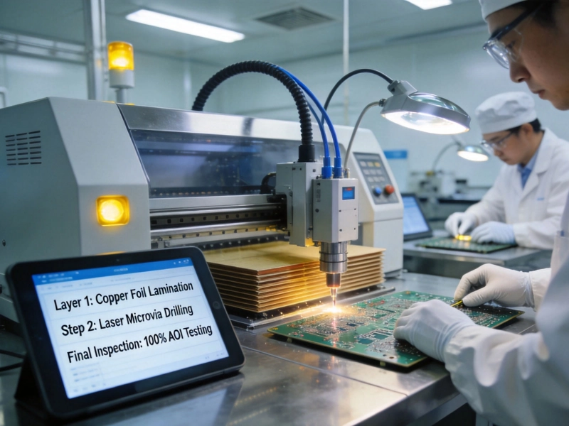
- Process specification: Detailed specification for HDI fabrication including microvia formation method (laser type, drilling parameters), plating processes, lamination cycles, and cleaning procedures. These must be locked down—uncontrolled process changes can alter biocompatibility and reliability outcomes.
- Reliability test results: IST data, thermal cycling data, moisture resistance data. Test samples must be representative of production boards—not specially prepared best-case samples.
- Change control: Any change to PCB materials, layer stack-up, via structure, or surface finish requires risk assessment and potentially re-testing. Medical device change control is not optional.
- Supplier qualification: The PCB fabricator must be qualified as a critical supplier. This means auditing their process controls, material traceability, and test capabilities—not just evaluating sample board quality.
FMEA for PCB Design Decisions
Failure Mode and Effects Analysis (FMEA) should be applied to PCB design decisions, not just to the device system level. Example FMEA entries for a medical HDI board:
- Failure mode: Microvia separation at capture pad interface. Effect: Open circuit in critical signal path, device malfunction. Cause: Insufficient plating adhesion due to excessive aspect ratio. Mitigation: Design rule limiting aspect ratio to 0.5:1, IST qualification to 1000+ cycles, incoming inspection sampling.
- Failure mode: Nickel ion leaching through porous gold plating. Effect: Cytotoxic response in patient tissue. Cause: Gold plating thickness below porosity threshold. Mitigation: Specify minimum 1.5 μm electroplated gold, verify with XRF thickness measurement on production boards.
- Failure mode: Moisture-induced delamination during sterilization. Effect: Via opens, device failure during reprocessing. Cause: Inadequate bake-out before lamination, excessive moisture absorption. Mitigation: Specify polyimide substrate, controlled storage conditions, pre-sterilization bake procedure.
This level of documentation may seem onerous, but it is the foundation of medical device safety. When a field event occurs, the DHF and FMEA are the first things regulators will request.
Key Takeaways
- Medical HDI boards require a fundamentally different design philosophy centered on risk management and patient safety, not just performance optimization.
- Material biocompatibility must be evaluated for the complete assembly—including substrates, surface finishes, solder mask, conformal coating, and any process residues.
- For implantable applications, halogen-free laminates, polyimide, or LCP substrates with ENEPIG or electroplated gold finishes provide the best biocompatibility profiles.
- Microvia Reliability is the critical concern for medical HDI—conservative aspect ratios, staggered via structures, copper fill, and aggressive thermal cycling qualification are non-negotiable.
- Cleanliness requirements for medical boards are 5–10× stricter than standard electronics, requiring enhanced cleaning processes and often cleanroom assembly.
- Electrical safety isolation requirements (IEC 60601-1 creepage and clearance) must be enforced from the earliest design stages, particularly in HDI boards where high via density can compromise isolation barriers.
- Sterilization compatibility must be validated for the specific method and cycle count the device will experience—there is no universal sterilization-compatible PCB design.
- Complete design traceability and risk documentation (DHF, FMEA) are regulatory requirements, not best practices.
Designing biocompatible and safe HDI boards for medical use is not simply a matter of specifying better materials and tighter tolerances. It requires a systematic approach that integrates biocompatibility assessment, reliability engineering, cleanliness control, electrical safety, and regulatory documentation into every design decision. The effort is significant—but when the result is a device that performs reliably inside a patients body for a decade without causing harm, the rigor is justified.
Contact us to discuss your requirements