Open Nav

Next-generation military radar and defense systems—from active electronically scanned array (AESA) radars and electronic warfare platforms to missile guidance systems and satellite communications terminals—require printed circuit boards that deliver extreme density, high-frequency performance, and unmatched reliability in the harshest operating environments. Traditional multilayer PCBs cannot meet the simultaneous demands for Miniaturization, high bandwidth, and ruggedization required for modern defense applications. Ruggedized High-density Interconnect (HDI) PCBs have emerged as the critical enabling technology for these systems, delivering 3-5x higher wiring density, superior Signal Integrity for millimeter-wave frequencies, and compliance with strict military reliability standards, all while reducing size and weight by up to 40% compared to conventional PCB designs.
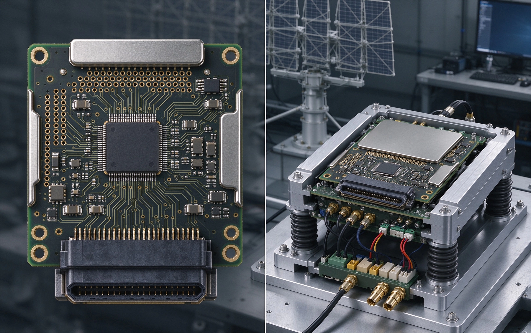
Defense electronics operate in some of the most extreme environments on (and off) Earth, with requirements far beyond those of commercial or even industrial applications:
Hdi Pcb technology uses Microvias (laser-drilled holes <150μm in diameter), blind and Buried Vias, and fine-line routing to achieve much higher wiring density than conventional multilayer PCBs. When optimized for defense applications with ruggedized materials and processes, HDI offers transformative benefits for military radar systems:
Modern AESA radars require thousands of individual T/R modules packed into a small array area. Ruggedized Hdi Technology supports routing densities up to 150 connections per square centimeter, 3-5x higher than conventional multilayer PCBs. This allows designers to fit entire T/R module circuits into form factors 50% smaller than previous generations, enabling larger, more capable radar arrays with more elements for higher resolution and longer detection range. HDI's Microvia Technology also eliminates the need for through-hole vias that block valuable routing space, enabling more efficient use of board real estate.
HDI's shorter signal paths and controlled impedance routing significantly reduce signal loss, crosstalk, and propagation delay compared to conventional PCBs, making it ideal for the millimeter-wave frequencies used in modern radar systems. The use of Microvias reduces parasitic inductance by up to 70% compared to through-hole vias, minimizing signal distortion at high frequencies. When paired with low-Dk/Df high-frequency materials like Rogers or Arlon laminates, ruggedized HDI PCBs can support signal frequencies up to 110GHz with Insertion Loss of less than 0.5dB per inch at 77GHz, meeting the strict performance requirements of next-generation radar systems.
For airborne, drone, and man-portable applications, every gram of weight saved directly improves mission capability. Ruggedized HDI PCBs can reduce the number of required board layers by 30-40% and reduce overall board size by up to 45% compared to conventional PCB designs, cutting total system weight by 30-50%. This weight reduction enables longer flight times for UAVs, increased payload capacity for fighter aircraft, and lighter, more man-portable radar systems for dismounted soldiers.
Ruggedized HDI PCBs are specifically engineered to withstand the extreme environments of defense applications. The use of microvias with plated copper filling eliminates the via cracking that is common with through-hole vias under thermal cycling and vibration. High-Tg (glass transition temperature) substrates, thick copper layers, and optional edge plating or stiffener frames improve mechanical strength, making Hdi Boards 2x more resistant to vibration and thermal cycling than conventional PCBs. Testing shows ruggedized Hdi Boards can survive over 1,500 thermal cycles from -55°C to +125°C without via or trace failures, meeting and exceeding MIL-STD-810 requirements.
Ruggedized Hdi Technology supports advanced integration features that are critical for defense applications, including embedded passive components (resistors, capacitors, filters) buried within the PCB layers, and even embedded active components. This eliminates the need for surface-mounted passives, reducing component count by up to 30%, improving Vibration Resistance, and reducing signal interference from exposed components. Embedded components also enable anti-tamper and anti-reverse engineering features, as critical circuitry is hidden within the board structure rather than visible on the surface.
Not all HDI PCBs are suitable for defense applications. Ruggedized military-grade HDI requires specialized materials, processes, and quality controls:
Every ruggedized Hdi Pcb for military radar applications undergoes extensive testing and qualification to ensure compliance with military standards:
We recently developed a ruggedized 8-layer HDI PCB for a next-generation airborne AESA fire control radar program for a U.S. defense prime contractor. The program's original conventional 14-layer Pcb Design was 40% over the weight limit, had 1.2dB of insertion loss at 35GHz, and failed vibration testing at 15g RMS.
Our ruggedized HDI solution delivered the following improvements:
The design has successfully completed qualification and is now in full production, with over 25,000 units deployed on multiple fighter aircraft platforms.
When selecting a supplier for ruggedized HDI PCBs for military radar and defense applications, ensure they meet these critical requirements:
Ruggedized Hdi Pcb Technology is the foundation of next-generation military radar and defense systems, enabling the higher performance, smaller size, and extreme reliability required for modern defense applications. Working with an experienced, certified defense PCB supplier ensures your radar systems meet all performance, reliability, and compliance requirements for successful deployment and decades of operational service.
Contact us to discuss your requirements.
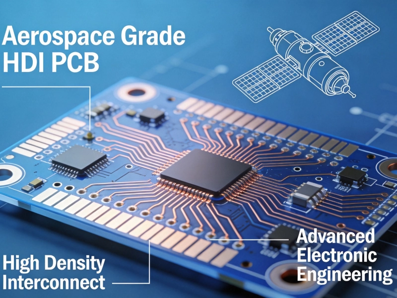
Designing HDI Boards to Withstand Extreme Aerospace EnvironmentsJuly/22/2026
High-Reliability Interconnects for Satellite and Space CommunicationSeptember/18/2026

HDI PCB Requirements for Mission-Critical Aerospace ApplicationsJune/30/2026
Selecting the Right Dielectric Materials for High-Performance HDI PCBsJune/05/2026

How HDI PCBs Power the Next Generation of SmartphonesJune/17/2026
Best Practices for BGA Fanout and Routing in HDI LayoutsJuly/07/2026
Copper Coin and Embedded Heat Sinks: Advanced Cooling for HDIJuly/08/2026
An Introduction to Microvia Technology in HDI PCBsJuly/24/2026