Open Nav

Modern electronic devices, from 5G communications equipment and high-performance computing systems to compact consumer electronics and automotive Adas Systems, are driving unprecedented demand for higher PCB density and faster signal speeds. Designers are packing more functionality into smaller form factors, leading to tighter trace spacing, thinner dielectric layers, and higher routing densities than ever before. At the same time, signal speeds are increasing to multi-gigabit rates, making even minor design imperfections a significant threat to Signal Integrity. Poor Signal Integrity in high-density designs can lead to data corruption, reduced performance, non-compliance with regulatory standards, and complete device failure. Understanding the common signal integrity challenges in high-density routing and how to address them is critical for designing reliable, high-performance electronic products.
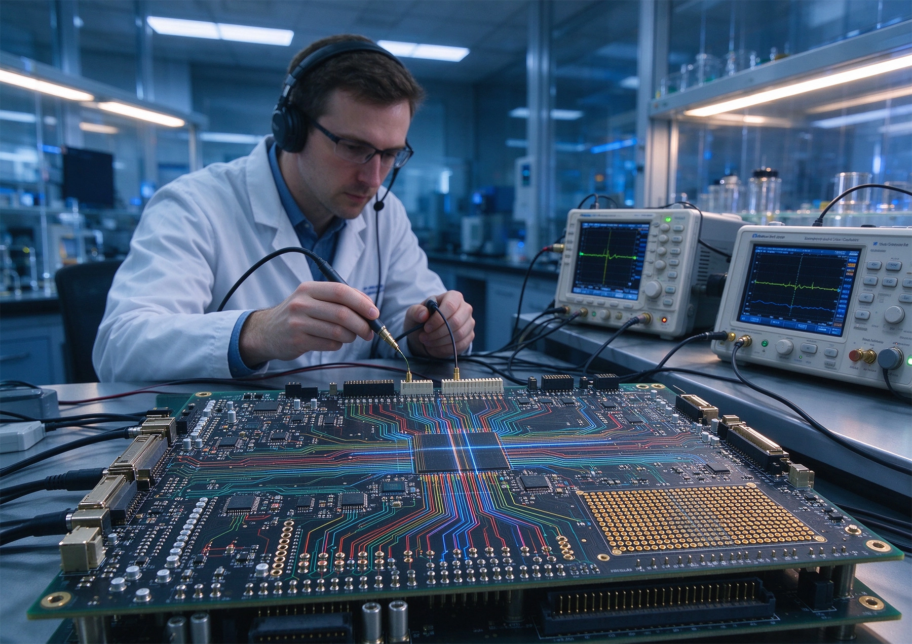
High-density PCB routing typically involves trace widths and spacing of 5mil or less, multiple high-speed signal layers, and large numbers of vias to connect components across layers. When signals operate at speeds of 1Gbps or higher, these design features interact with the electrical properties of the PCB material to create signal integrity issues that are negligible at lower speeds. Even a 10% error in signal voltage or a few picoseconds of timing error can cause a high-speed link to fail completely. As signal speeds continue to increase and form factors shrink, signal integrity has become one of the primary limiting factors in high-density Pcb Design.
These are the most prevalent signal integrity challenges designers face in high-density PCB designs:
Crosstalk is the unintended electromagnetic coupling between adjacent signal traces. When high-speed signals travel through a trace, they generate electromagnetic fields that can induce unwanted voltages in adjacent traces. In high-density designs with tight trace spacing, crosstalk becomes a significant problem, leading to signal distortion, increased noise margins, and data errors. There are two types of crosstalk: far-end crosstalk (FEXT) which travels in the same direction as the aggressor signal, and near-end crosstalk (NEXT) which travels in the opposite direction.
Crosstalk risk increases as trace spacing decreases and signal speeds increase, making it one of the most common signal integrity issues in high-density designs. In severe cases, crosstalk can induce enough noise in a victim trace to cause false triggering of logic circuits or complete data corruption.
High-speed signals require controlled impedance along the entire signal path to ensure maximum power transfer and minimum signal reflection. Any change in the impedance of the signal path causes a portion of the signal to be reflected back toward the source, leading to signal distortion, reduced signal amplitude, and timing errors. In high-density designs, impedance discontinuities are commonly caused by:
For high-speed signals operating at 10Gbps or higher, even small impedance discontinuities of 5-10 ohms can cause enough reflection to degrade signal quality below acceptable levels.
Many high-speed interfaces use differential signaling or parallel data buses that require precise timing alignment between signal pairs or across multiple data lines. Timing skew occurs when signals that should arrive at the same time arrive at different times due to differences in trace length, material properties, or routing geometry. In high-density designs, routing constraints often force designers to route signals around obstacles, leading to length mismatches between related signals.
Excessive timing skew can cause setup and hold time violations, leading to data errors and reduced link performance. For high-speed differential interfaces such as PCIe 5.0 or USB4, even a few picoseconds of skew between differential pairs can cause link failure.
High-speed signals in dense routing environments generate significant electromagnetic radiation that can cause interference with other circuits and lead to failure to meet regulatory EMC standards. The tight trace spacing and high routing density of modern designs increase the risk of both radiated emissions (energy emitted from the PCB) and susceptibility (the PCB being affected by external radiation). Common sources of EMI in high-density designs include unshielded high-speed signal traces, poor return path design, and improper grounding.
Insertion Loss is the reduction in signal power as it travels through the transmission line, caused by a combination of conductor resistance, Dielectric Loss, and radiation loss. In high-density designs, signals often have to travel longer routes through narrow traces, increasing conductor loss. At multi-gigabit speeds, Dielectric Loss from the PCB substrate material becomes a significant factor, further attenuating high-frequency signal components. Excessive Insertion Loss reduces the signal-to-noise ratio at the receiver, leading to increased bit error rates and reduced link reach.
These design strategies address the signal integrity challenges of high-density routing while maintaining high routing density:
Follow these best practices to ensure signal integrity in your high-density designs:
Signal integrity is a critical consideration in high-density Pcb Design, especially as signal speeds continue to increase and form factors shrink. By understanding the common signal integrity challenges of high-density routing and implementing proven design solutions, you can ensure your high-speed designs deliver reliable performance while meeting size and density requirements. The key to success is addressing signal integrity early in the design process, using simulation tools to validate performance, and following established design best practices for controlled impedance, crosstalk reduction, timing management, and EMI control. With careful planning and attention to detail, you can overcome the signal integrity challenges of high-density routing and design high-performance electronic products that meet all reliability and performance requirements.
Contact us to discuss your requirements.
A: High-density routing is typically defined as designs with trace widths and spacing of 5mil (0.127mm) or less, multiple signal layers, and high via density.
A: Signal integrity becomes a consideration for signals with rise times faster than 1ns, which typically corresponds to data rates of 1Gbps or higher. For slower signals, signal integrity issues are usually negligible.
A: The 3W rule (spacing of 3x the trace width) is a good general guideline. For very high-speed signals, increase spacing to 5x the trace width for additional isolation.
A: Use electromagnetic simulation tools to perform signal integrity analysis, including impedance analysis, crosstalk simulation, and eye diagram analysis to predict performance before manufacturing.
A: Minor signal integrity issues can sometimes be fixed with firmware adjustments or component changes, but most significant issues require a PCB redesign. It is far more cost-effective to address signal integrity during the design stage.
High-Reliability HDI Solutions for PLCs and Motor DrivesSeptember/16/2026

HDI PCBs in Industrial IoT (IIoT) and Smart Factory SensorsJune/29/2026

Partnering with a China Manufacturer for Your High-End Industrial SMT ProjectsOctober/19/2026
Designing Rugged HDI Boards for Harsh Industrial EnvironmentsJuly/20/2026
The Impact of Via-in-Pad on Thermal Performance and ReliabilitySeptember/26/2026
Understanding the Core Differences Between HDI and Traditional PCBsJuly/02/2026
What is High Density Interconnect (HDI) PCB?May/28/2026
Troubleshooting Common Issues in HDI PCB AssemblySeptember/09/2026