Open Nav

Industrial automation equipment operates in environments that test the limits of electronic hardware. Factory floors subject PCBs to temperature extremes that swing between the heat of running machinery and the chill of shutdown periods, vibration that stresses every solder joint and via barrel, and contamination that accelerates corrosion on exposed conductor surfaces. Within these environments, High-density Interconnect boards—the compact, densely routed PCBs that pack sophisticated control and communication functionality into minimal space—face thermal stress challenges that are amplified by their very architecture. The Microvias, fine traces, and thin dielectrics that enable HDI density also create vulnerability points where thermal stress concentrates, and a failure at any one of these points can disable an entire control module. Managing thermal stress in industrial automation Hdi Boards is therefore not a secondary design consideration but a primary reliability requirement that must be addressed from material selection through layout design and manufacturing process control.
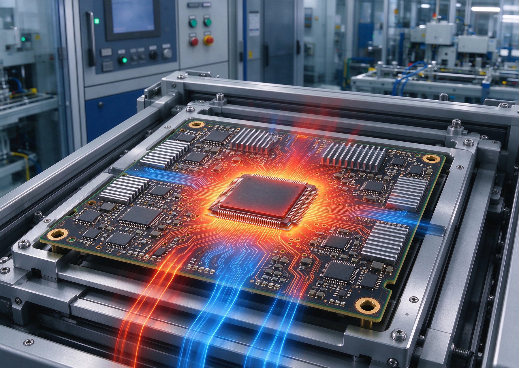
Thermal stress in industrial Hdi Boards originates from multiple sources that often act simultaneously. External ambient temperature cycling drives the board through temperature swings that can span fifty degrees Celsius or more between equipment operating and idle states. Internal heating from power devices—motor drivers, power converters, and communication transceivers—creates localized hot spots that subject the surrounding board structure to steep thermal gradients. Reflow assembly itself imposes the most severe thermal excursion the board will ever experience, with peak temperatures exceeding 245 degrees Celsius for lead-free profiles that stress the laminate, the via structures, and every material interface on the board.
The coefficient of thermal expansion mismatch between the materials that compose an HDI board is the fundamental driver of thermomechanical stress. Copper expands at roughly 17 parts per million per degree Celsius, while FR-4 laminate expands at 14 to 18 ppm in the x-y plane but can expand at 50 to 70 ppm in the z-axis perpendicular to the board surface. This Cte Mismatch creates shear stress at every copper-to-substrate interface, tensile stress in via barrels during heating, and compressive stress during cooling. Over many thermal cycles, the accumulated fatigue from these alternating stresses degrades material interfaces, cracks via barrels, and eventually produces electrical opens or intermittent connections that cause field failures.
HDI construction intensifies these challenges because Microvias—the small laser-drilled or mechanically drilled holes that connect adjacent layers in HDI buildups—are inherently more vulnerable to thermal fatigue than conventional through-hole vias. Their smaller diameter means less copper cross-section to carry current and resist mechanical stress, and their placement in sequential build-up layers means they are embedded in thinner dielectric sections that experience greater strain during thermal cycling. A Microvia that cracks under thermal stress can disable a critical signal path or power connection with no external indication of the failure.
The laminate material is the first and most fundamental line of defense against thermal stress. Standard FR-4 formulations with glass transition temperatures around 130 to 140 degrees Celsius provide insufficient margin for industrial applications where operating temperatures may approach or exceed 100 degrees Celsius and where assembly reflow peaks push the material close to its decomposition threshold. Selecting a High-tg Laminate with a glass transition temperature of 170 degrees Celsius or higher provides the thermal headroom needed to survive both assembly and field thermal cycling without approaching the transition region where the material's mechanical properties degrade rapidly.
Mid-loss and low-Df materials that offer improved electrical performance for high-speed signals also tend to deliver better thermal stability because their resin systems incorporate higher cross-link density and more thermally robust chemistry. However, the tradeoff is that some high-performance formulations exhibit higher stiffness that can increase the stress transferred to via structures during thermal cycling. The material selection process should balance thermal headroom, mechanical compliance, and the electrical performance requirements of the specific design rather than simply maximizing any single parameter.
Z-axis CTE is the material property most directly relevant to via reliability under thermal cycling. Laminates with lower z-axis CTE produce less differential expansion between the via barrel and the surrounding substrate, reducing the cyclic shear stress that drives fatigue cracking. Filled via materials—both copper-filled microvias and resin-filled via structures—help by providing a more compliant interface that accommodates some of the differential strain, but the fundamental stress level is set by the laminate's CTE behavior.
Microvia Reliability under thermal cycling is one of the most studied and discussed topics in Hdi Manufacturing, and the design practices that emerge from this body of knowledge are critical for industrial automation boards that must survive years of thermal cycling in the field. The key risk factors for Microvia failure are aspect ratio, via Copper Plating quality, landing pad design, and the specific stacking arrangement used in the HDI buildup.
Aspect ratio—the ratio of via depth to via diameter—should be kept below 1.0 for microvias whenever possible. Higher aspect ratios make it more difficult to achieve uniform Copper Plating through the full depth of the via, and Plating Voids or thin spots at the via barrel become nucleation points for fatigue cracks. A microvia with an aspect ratio of 0.75 or less can be reliably plated with consistent copper thickness, providing the mechanical cross-section needed to resist thermal cycling fatigue.
Staggered via structures, where microvias on adjacent layers are offset so they do not align vertically, are preferred over Stacked Microvias for thermally demanding applications. Stacked vias—where a microvia on one layer lands directly on top of a microvia on the layer below—create a continuous copper column that is more susceptible to crack propagation because a crack that initiates at one via interface can propagate through the entire stack. Staggered structures interrupt this crack path and distribute the thermal strain across separate via locations, improving overall reliability. When stacked vias are necessary for routing density, target pad design—enlarging the pad at the via transition point—reduces the stress concentration at the critical interface.
Copper filling of microvias provides superior current carrying capacity and improved Thermal Conductivity compared to open or tented vias, and the filled structure is more resistant to fatigue cracking because the copper fill eliminates the void space where stress concentrates at the via barrel-to-pad interface. IPC-4761 Type VII filled and capped vias represent the most robust construction for microvias in thermally demanding applications, providing both electrical reliability and a planar surface suitable for component mounting on the via pad.
Thermal stress in a Multilayer Pcb is influenced by the distribution of copper across the board and across the layer stack. Uneven copper distribution creates warpage during thermal excursions because regions with different copper densities expand and contract at different rates, bending the board and stressing the via and interconnect structures that hold it together. In HDI boards for industrial applications, where reliability margins must be maintained over extended service lives, copper balancing is not optional—it is a design requirement.
Symmetrical stackup design—arranging the layer stack so that the copper distribution and material thicknesses are mirrored about the board centerline—minimizes the warpage that occurs during both assembly reflow and field thermal cycling. An unbalanced stackup warps predictably when heated because one side of the board expands more than the other, and this warpage stresses every via, every solder joint, and every material interface in the structure. Maintaining symmetry eliminates the root cause of this warpage mode and the cascade of stresses it produces.
Copper thieving—adding non-functional copper features to outer layers to balance the copper density against the inner layer planes—is a standard practice that should be applied systematically to Industrial Hdi boards. The goal is to ensure that the average copper coverage on each layer is similar, so that no layer acts as a significantly different thermal expansion driver relative to its neighbors. Modern CAD tools provide copper balancing analysis that quantifies the distribution across layers and identifies areas where additional balancing copper would improve uniformity.
Components that dissipate significant power—motor driver ICs, power MOSFETs, and DC-DC converters—create localized hot spots that subject the surrounding board structure to thermal gradients far more severe than the ambient temperature cycling the whole board experiences. Thermal Vias placed beneath and around these components provide a conductive path that spreads heat from the component into the internal copper planes and ultimately to the board surface or mounting hardware where it can be dissipated to the environment.
The design of thermal via arrays requires attention to both Thermal Performance and reliability. More vias provide better thermal conductance, but each via represents a potential reliability risk point under thermal cycling. The via diameter, plating thickness, and fill method all affect both the thermal resistance of the via and its fatigue life. Filled Thermal Vias provide the lowest thermal resistance and the highest reliability, but at a manufacturing cost premium that must be justified by the Thermal Management requirement. For many industrial applications, the cost of filled vias is justified by the improvement in both Thermal Performance and long-term reliability.
The placement of thermal vias relative to component solder pads affects both thermal performance and assembly yield. Vias in pad—where thermal vias are placed directly within the component solder pad—provide the shortest thermal path from the component to the internal planes but can cause solder wicking into the via during reflow, reducing the solder volume available for the joint. This issue is managed by filling and capping the vias before assembly or by using Via-in-pad construction with tenting that prevents solder intrusion. For industrial applications where reliability cannot be compromised, filled and capped Via-in-pad is the recommended approach despite the additional processing cost.
Solder joints are among the most vulnerable interconnect structures in an HDI assembly under thermal cycling, and the combination of HDI density—fine-pitch components, small passive devices, and BGA packages with many solder balls—creates a large population of joints that must all survive the full thermal cycling life of the product. The reliability of each joint depends on its geometry, the component and pad materials, the solder alloy, and the thermal strain it experiences, which varies across the board depending on the local thermal environment and the distance from the neutral point of the assembly.
Lead-free solder alloys, now mandated by environmental regulations, exhibit different fatigue characteristics than the tin-lead alloys they replaced. SAC305 and similar SAC-family alloys have higher melting temperatures and different creep behavior that produces different fatigue life under thermal cycling. In general, lead-free solder joints are more resistant to high-strain cycling but can be more susceptible to low-strain, high-cycle fatigue that accumulates over many thousands of mild temperature excursions. Understanding the specific cycling profile your product will experience in the field—temperature range, cycle frequency, dwell times at temperature extremes—allows reliability predictions that guide design decisions about component placement, solder volume, and the use of corner staking or underfill for BGA components.
For BGA components mounted on HDI boards, underfill provides significant improvement in solder joint reliability by distributing the thermal mismatch strain between the component and the board across the entire component footprint rather than concentrating it in the outermost solder balls. In industrial automation applications where BGAs are used for processors, FPGAs, or communication controllers, underfill is strongly recommended for any component whose failure would disable the control function. The underfill material must be selected for compatibility with the operating temperature range and for its own CTE, which should bridge the gap between the component substrate and the board laminate to provide the most uniform strain distribution.
Predicting thermal stress performance before hardware is built allows design improvements at a stage when changes are inexpensive. Thermal Simulation tools model the temperature distribution across the board under operating conditions, identifying hot spots, thermal gradients, and regions where the temperature exceeds the rated limits of the laminate or components. These simulations should incorporate the actual power dissipation of all components, the Thermal Conductivity of the board stackup including via arrays, and the convection conditions that represent the installed environment—whether the board is in a sealed enclosure, a forced-air cooled rack, or an open chassis with natural convection.
Thermomechanical simulation extends thermal analysis to predict the stress and strain in the board structure that results from the temperature distribution. These simulations can identify via locations where the cyclic stress exceeds the fatigue endurance limit of the via structure, solder joints where the accumulated strain will produce cracking within the target product life, and regions of the board where warpage will stress interconnects. While thermomechanical simulation requires significant modeling effort and material property data, it provides insight that is impossible to obtain from prototype testing alone because it reveals the stress state inside the board structure where failures originate.
Physical validation through thermal cycling testing confirms that the design meets its reliability targets under real or accelerated thermal cycling conditions. Ipc-9701 provides a framework for thermal cycling test conditions, acceptance criteria, and the use of Weibull statistical analysis to project field reliability from test data. For industrial automation boards, thermal cycling to Ipc-9701 TC3 or more severe conditions, with sufficient cycle count to establish a statistically meaningful failure distribution, provides the evidence needed to release the design for production with confidence in its field reliability.
What is the recommended maximum aspect ratio for microvias in thermally demanding applications?
An aspect ratio below 1.0 is strongly recommended, with 0.75 or lower preferred for the highest reliability. Lower aspect ratios enable more uniform copper plating and reduce the stress concentration at the via barrel.
Are Stacked Microvias ever acceptable for industrial automation boards?
Stacked vias can be used when routing density requires them, but they should be limited in number and designed with target pads that reduce stress at the via transition interface. Staggered structures should be used wherever the routing permits, as they provide superior resistance to crack propagation under thermal cycling.
How does copper filling improve microvia reliability?
Copper filling eliminates the void space inside the via where stress concentrates at the barrel-to-pad interface, provides additional mechanical cross-section to resist fatigue, and improves thermal conductivity through the via structure. IPC-4761 Type VII filled and capped construction offers the highest reliability for thermally demanding applications.
What thermal cycling test conditions should be used for industrial automation HDI boards?
IPC-9701 TC3 conditions, typically 0 to 100 degrees Celsius or -40 to 125 degrees Celsius depending on the expected field environment, with sufficient cycles to establish a Weibull failure distribution that projects to the target field life with statistical confidence.
Is underfill always necessary for BGA components on industrial HDI boards?
Underfill is strongly recommended for any BGA whose failure would disable a critical function. For non-critical BGAs in benign thermal environments, underfill may be optional, but the risk assessment should consider the full thermal cycling profile and the difficulty of rework on HDI construction where microvia damage during BGA removal is a concern.
Contact us to discuss your requirements and learn how our Hdi Manufacturing expertise supports reliable board production for demanding industrial automation thermal environments.
How to Use Thermal Simulation Software to Optimize HDI LayoutsJuly/29/2026
Copper Coin and Embedded Heat Sinks: Advanced Cooling for HDIJuly/08/2026
Exploring the 6 Types of HDI Structures: From Type I to Any-LayerAugust/14/2026
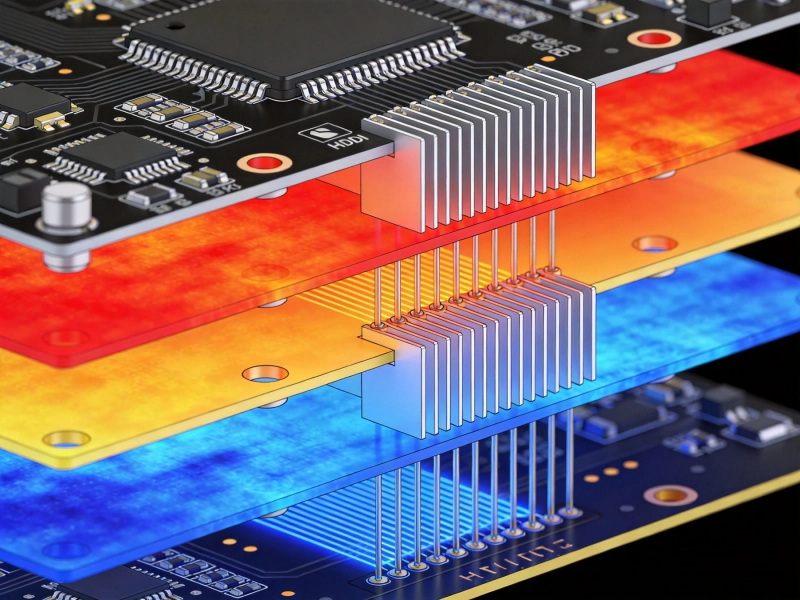
Effective Thermal Management Strategies for High-Density PCBsMay/28/2026
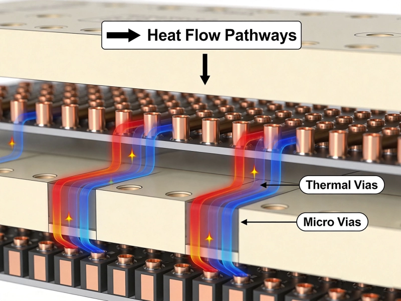
The Role of Thermal Vias in Dissipating Heat from HDI BoardsJune/09/2026
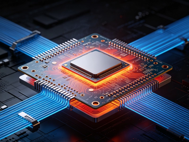
Managing Heat in High-Power HDI Applications: A Practical GuideSeptember/03/2026
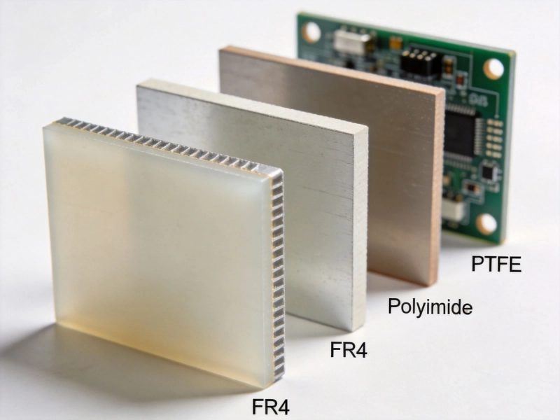
Selecting the Right Dielectric Materials for High-Performance HDI PCBsMay/28/2026
The Impact of Via-in-Pad on Thermal Performance and ReliabilitySeptember/26/2026