Open Nav

Heat is the enemy of electronics reliability. As PCB designs grow denser and power densities increase, managing Thermal Performance moves from an afterthought to a primary design constraint. In Hdi Boards, where Microvia densities are high and component Miniaturization pushes power into smaller footprints, Thermal Management is not optional; it is foundational to getting the product to work and keeping it working. Understanding how different HDI material options affect Thermal Conductivity gives engineers the information needed to make material choices that support both electrical performance and thermal survival.
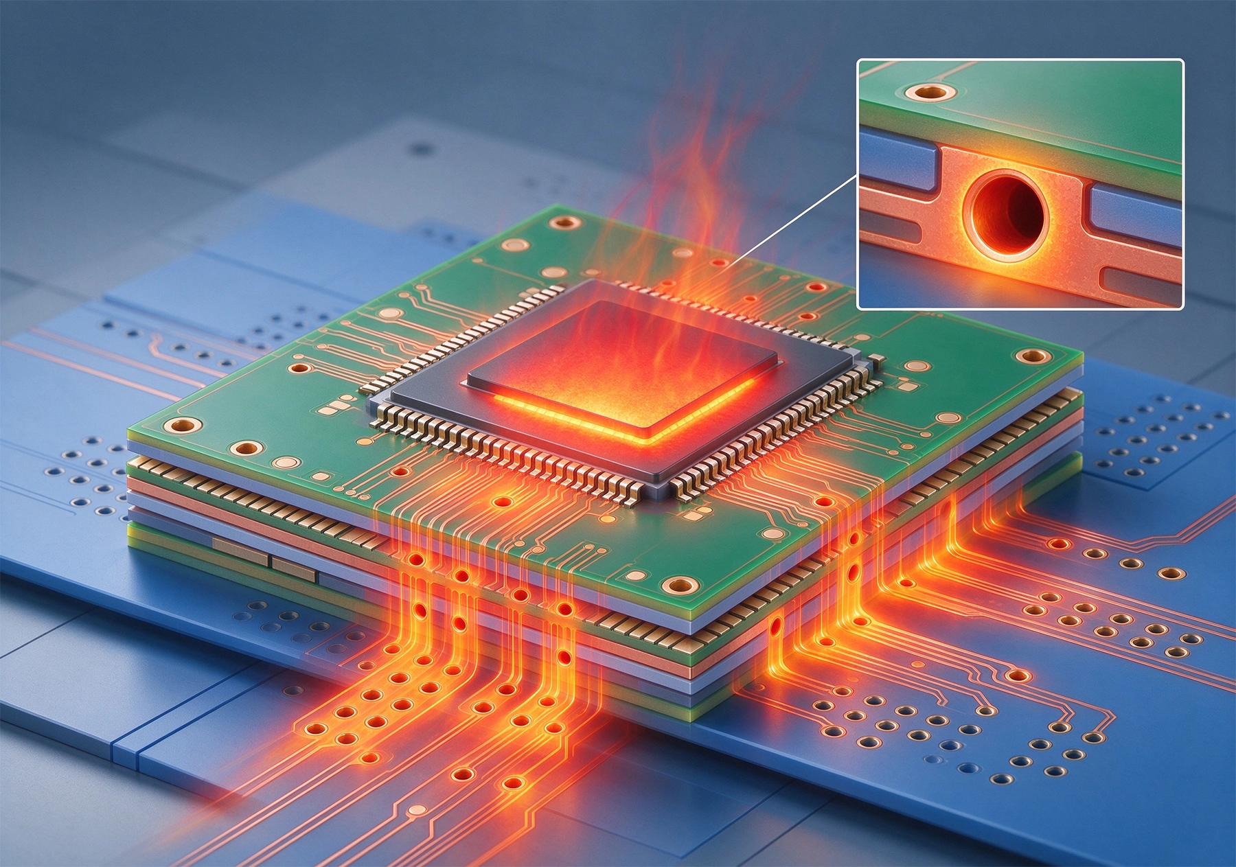
Hdi Boards concentrate more functionality into smaller areas than conventional multilayer designs, which means the heat generated per unit area is typically higher. A modern smartphone processor, for example, dissipates several watts from a chip that measures a few millimeters on a side. The thermal path from that chip through the PCB to the surrounding environment must handle heat fluxes that would have been considered extreme even a decade ago.
The Thermal Conductivity of the PCB substrate determines how efficiently heat spreads from the heat-generating component through the board. A substrate with low thermal conductivity acts as a thermal bottleneck, causing localized hotspots that degrade component performance and lifespan. A substrate with higher thermal conductivity spreads the heat more effectively, reducing the peak temperature at the source and moving the thermal load closer to the board edges where it can dissipate into the surrounding environment.
In conventional FR-4 substrates, thermal conductivity is approximately 0.3 watts per meter-kelvin, which is essentially that of the fiberglass reinforcement and epoxy resin system. This is low by any engineering standard. When a high-power component is mounted on a standard FR-4 board, most of the Heat Dissipation occurs through the copper planes and traces rather than through the dielectric, and the dielectric itself provides significant thermal resistance. For HDI boards used in high-power applications, this limitation is unacceptable, and designers must look to alternative materials with higher thermal conductivity.
The Hdi Manufacturing ecosystem includes several material families, each with different thermal conductivity characteristics. Understanding the options and their trade-offs is the starting point for making informed material decisions.
Standard FR-4 remains the baseline material for many Hdi Applications, particularly those where power dissipation is modest and cost is the primary driver. The thermal conductivity of standard FR-4, while low, has been improved in some high-Tg formulations through the addition of thermally conductive fillers. These filled FR-4 materials can achieve thermal conductivity in the range of 0.5 to 1.0 W/mK, which is a meaningful improvement over unfilled material, though still far below what is achievable with specialized thermal materials.
Polyimide-based materials, including flex and rigid-flex HDI constructions, offer moderate improvements in thermal conductivity over standard FR-4 and bring superior thermal cycling performance. The polyimide resin system has a thermal conductivity around 0.5 W/mK, and polyimide boards can sustain higher continuous operating temperatures, which partially compensates for the limited thermal conductivity by allowing higher absolute operating temperatures before thermal degradation becomes a concern.
BT (bismaleimide triazine) resin systems, used in many Hdi Applications for their excellent electrical properties and processing stability, have thermal conductivity characteristics similar to standard FR-4, in the range of 0.3 to 0.5 W/mK depending on the specific formulation and filler content. BT is often selected for its low Dielectric Loss and good dimensional stability rather than its thermal properties, and boards using BT as the primary dielectric typically rely on copper planes and Thermal Vias for heat spreading rather than the dielectric itself.
For applications where Thermal Management is a critical requirement, several substrate options offer substantially higher thermal conductivity than standard HDI materials. These materials come with their own trade-offs in cost, processability, and electrical properties, and understanding these trade-offs is essential to making appropriate material selections.
Metal core substrates, typically built on aluminum or copper cores with a dielectric layer and circuit pattern on one or both sides, offer thermal conductivity dominated by the metal core, which ranges from 150 W/mK for aluminum to over 400 W/mK for copper. The dielectric layer in a metal core construction is thin, often in the range of 50 to 150 microns, which minimizes the thermal resistance of the dielectric itself. Metal core boards are widely used in LED lighting, power conversion, and other high-power applications where the thermal path from the component to the metal core is the primary Heat Dissipation mechanism.
Insulated metal substrate (IMS) construction extends the metal core concept to multilayer HDI designs. An IMS board uses a dielectric layer with high thermal conductivity, typically 1 to 5 W/mK, between the circuit layer and the metal base. The dielectric is designed to provide both electrical isolation and thermal conduction, and the combination of a thin dielectric layer with high thermal conductivity and a metal base with excellent heat spreading makes IMS an effective solution for thermal management in Power Electronics applications.
Ceramic substrates, including alumina (Al2O3) and aluminum nitride (AlN), offer thermal conductivity ranging from 20 W/mK for alumina to over 180 W/mK for aluminum nitride. These materials are used in specialized applications like RF power amplifiers, Automotive Electronics, and aerospace systems where both Thermal Performance and excellent electrical insulation are required. Ceramic substrates are significantly more expensive than organic-based materials and are typically used only when the thermal and electrical performance requirements justify the cost.
Regardless of the base substrate material, Thermal Vias are one of the most powerful tools available for managing heat in HDI boards. A thermal via is a via structure that is specifically designed to conduct heat from a component pad or plane on one layer to a larger copper area on another layer, typically a metal core or a large ground plane connected to a heatsink. The thermal performance of a properly designed thermal via array can exceed what is achievable through the dielectric alone by orders of magnitude.
The thermal conductivity of a filled thermal via can reach 10 to 20 W/mK or higher depending on the fill material and via geometry. This is achieved by plating the via barrel with copper, which has a thermal conductivity of approximately 385 W/mK, or by filling the via with thermally conductive epoxy or solder. The key to effective thermal via design is adequate via density, appropriate via diameter, and sufficient Copper Plating thickness to provide a low-resistance thermal path.
In HDI designs, thermal vias are often integrated directly into the component pad structure, with the via placed in the center or near the center of the pad to minimize the thermal resistance from the component to the thermal structure. Via-in-pad construction, which is standard in many HDI applications, naturally supports this approach. For high-power components like processors, memory packages, and power transistors, a grid of thermal vias under the component footprint is a standard practice that significantly improves thermal performance.
The effectiveness of a thermal via array is also determined by the thermal interface between the via array and the heat sink or mounting structure. A thermal via array that terminates at a Thermal Pad on the board surface, which is then mated to a heatsink with thermal interface material, is far more effective than one that terminates at an internal plane with no path to the external environment. In HDI designs where component density limits access to the board surface, thermal vias may need to extend through multiple layers to reach an exposed Thermal Pad, which adds to the design complexity and requires careful stackup planning.
Designing thermal management into an HDI board without simulation is like designing RF circuits without network analysis: it can be done, but the results are uncertain and the process is inefficient. Thermal Simulation, using finite element analysis tools or dedicated PCB thermal analysis software, allows the engineer to evaluate different material and via configurations, predict temperature distributions under specified power loads, and optimize the thermal design before committing to fabrication.
The accuracy of Thermal Simulation depends on having accurate material property data for the components, the substrate, and the thermal interface materials. For many commercial HDI materials, thermal conductivity data is available from the material datasheet, but the effective thermal conductivity in the board context may differ from the raw material property due to variations in resin content, void content, and the effect of glass weave distribution in fiberglass-reinforced materials. When datasheet values are uncertain, measurement of representative test structures can provide calibration data that improves simulation accuracy.
Thermal measurement of prototype boards provides the validation data needed to confirm that the design meets its thermal targets. Infrared thermography is a non-contact method for mapping surface temperatures on an operating board, which can reveal hot spots that were not predicted by simulation. Thermocouple measurement provides point temperature data at specific locations, which is useful for verifying simulation predictions at critical points like component junctions and thermal pads. Both methods should be used during prototype validation to confirm thermal design performance and identify any issues that require design modification.
In practice, material selection for thermal management in HDI designs involves balancing multiple factors, and there is rarely a single optimal choice. Cost is almost always a factor: materials with higher thermal conductivity typically cost more, and the cost premium must be justified by the performance improvement. Processability affects which manufacturers can produce the board reliably and may influence design rules, minimum feature sizes, and yield expectations. Electrical properties, including dielectric constant and loss tangent, interact with thermal properties because some high-thermal-conductivity materials have electrical properties that are less suitable for high-frequency or high-speed signal transmission.
A practical approach to material selection starts with identifying the thermal constraint that is most critical for the application. If the primary concern is junction temperature of a high-power component, focus on thermal via design and thermal interface materials as the first line of defense, and evaluate higher-conductivity substrates only if those measures are insufficient. If the primary concern is heat spreading across a large board area, a metal core or IMS substrate may be the most effective solution. If the primary concern is thermal cycling reliability, material systems with low coefficient of thermal expansion and good fatigue resistance may take precedence over raw thermal conductivity.
Collaboration with the PCB fabricator is essential for material selection decisions that involve non-standard materials. The fabricator's process capabilities determine which material options are actually available, and their experience with specific material systems provides practical guidance on process parameters, yield expectations, and potential issues. A material that looks attractive on paper may be difficult to process reliably in production, and the fabricator is the best source of information about these practical constraints before the design is finalized.
The thermal management challenge in HDI designs continues to intensify as component power densities increase and product form factors become more constrained. The materials industry is responding with new substrate options that push thermal conductivity higher while maintaining the processability and cost profile needed for high-volume applications.
Thermally enhanced epoxy systems with ceramic filler loadings are becoming more common in HDI applications. These materials achieve thermal conductivity in the range of 1 to 3 W/mK through high filler loadings of alumina, silica, or boron nitride, while maintaining processing characteristics that are compatible with standard PCB Fabrication methods. The trade-off is typically higher dielectric constant and some reduction in flexural strength or thermal cycling performance compared to unfilled systems, but for applications where thermal performance is the primary constraint, these trade-offs are often acceptable.
Graphite-based thermal substrates represent an emerging option for ultra-high thermal conductivity applications. Graphite has an in-plane thermal conductivity that can exceed 1000 W/mK, orders of magnitude higher than any polymer composite. Graphite thermal substrates, typically constructed as a thin graphite core sandwiched between dielectric layers and copper foils, can achieve thermal conductivity performance approaching metal core substrates while maintaining a thin, lightweight form factor. The challenges for these materials include electrical isolation requirements, mechanical robustness, and integration with standard PCB assembly processes, but several manufacturers are actively developing products that address these challenges.
Diamond-filled composite substrates, which use synthetic diamond particles as a thermal filler in a polymer matrix, offer the highest thermal conductivity available in an organic substrate format, potentially exceeding 10 W/mK. These materials are currently in early adoption stages for the most demanding thermal applications, where the cost premium is justified by performance requirements that cannot be met by any other available material. As manufacturing scale increases and costs decrease, diamond-filled composites may become more widely available for mainstream high-power HDI applications.
Thermal conductivity in HDI materials is a critical design parameter that deserves the same careful attention as electrical performance, cost, and manufacturability. The range of available options, from standard FR-4 at 0.3 W/mK to diamond-filled composites at over 10 W/mK, spans more than an order of magnitude in thermal performance and represents a corresponding range of cost and processability trade-offs. Making appropriate material selections requires understanding the thermal requirements of the specific application, evaluating the available material options against those requirements, and engaging the fabricator early to validate that the chosen materials can be processed reliably.
The most effective thermal management strategies for HDI designs combine multiple approaches: appropriate substrate selection, strategic use of thermal vias, effective thermal interface materials, and thermal simulation during the design phase to validate the approach before fabrication. None of these elements alone is sufficient for demanding thermal applications, but together they provide a systematic framework for addressing thermal challenges in high-density designs. As component power densities continue to increase, the importance of this systematic approach to thermal management will only grow.
Contact us to discuss your requirements.
Selecting the Right Dielectric Materials for High-Performance HDI PCBsJune/05/2026
FR-4 vs. High-Tg Materials: What Works Best for HDI Applications?July/07/2026
Managing Layer-to-Layer Registration Accuracy in Multilayer HDIOctober/09/2026
Understanding the Role of Copper Foil Roughness in Signal IntegritySeptember/23/2026
Essential HDI PCB Design Rules for Beginners and ExpertsMay/28/2026
What is High Density Interconnect (HDI) PCB?May/28/2026
An Introduction to ABF (Ajinomoto Build-up Film) for Advanced HDIJuly/27/2026
Why Low Loss Materials are Critical for High-Speed HDI DesignsSeptember/01/2026