Open Nav

High-density Interconnect PCBs present inspection challenges that traditional manual approaches struggle to address consistently. The microscopic features, dense component placement, and tight tolerances of Hdi Boards demand inspection methods that can match human expertise while maintaining the consistency and speed that modern production volumes require. Automated Optical Inspection has emerged as the primary solution for these challenges, but implementing AOI effectively in HDI production requires more than simply purchasing a machine and placing it on the production line.
This article examines the practical considerations for integrating AOI into Hdi Manufacturing operations. Whether you are evaluating AOI for the first time or looking to improve the performance of an existing AOI system, understanding how these systems work, what they can detect, and where they struggle helps you get maximum value from your inspection investment.
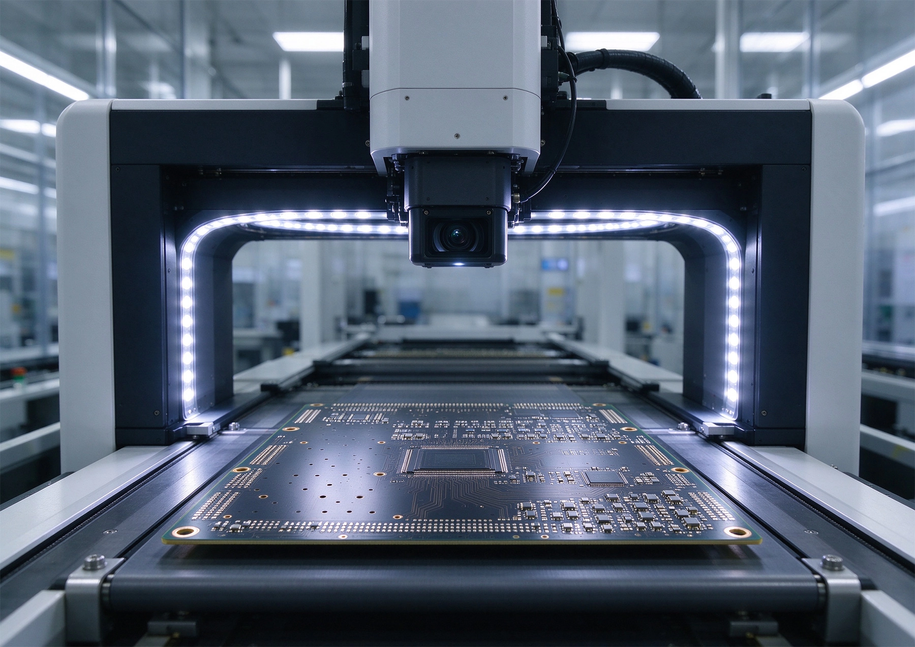
AOI systems use cameras and image analysis software to inspect PCBs for defects after assembly. The basic workflow involves illuminating the board surface, capturing images with sufficient resolution to see relevant features, and comparing those images against reference data that defines what a good board looks like. Any significant deviation from the reference triggers a defect alert that operators review to determine whether the board actually has a problem.
Modern AOI systems employ multiple lighting techniques to highlight different defect types. Bright field illumination, where light reflects directly back toward the camera, works well for detecting missing components, component misalignment, and solder bridges. Dark field illumination, where light reflects at sharp angles, reveals surface irregularities like scratches, pits, and insufficient solder coverage. Many systems alternate between lighting modes or use multiple simultaneous lighting configurations to maximize defect detection across all relevant failure modes.
Image analysis algorithms have advanced significantly beyond simple pixel-by-pixel comparison. Modern systems use statistical analysis to distinguish between normal manufacturing variation and actual defects, reducing false call rates that waste inspection time on boards that are actually good. Some systems employ machine learning to improve detection accuracy based on examples of known defects and acceptable boards from your specific production process.
Hdi Manufacturing creates inspection challenges that are fundamentally different from conventional PCB assembly. Understanding these challenges helps explain why AOI implementation in HDI production requires more careful planning than it might for simpler board types.
Component Miniaturization means that features are smaller and closer together than in conventional designs. 01005 passives and micro-BGA packages have tolerances measured in hundredths of a millimeter, requiring imaging resolution that strains the limits of standard AOI systems. A camera that provides adequate resolution for 0603 components may miss defects on much smaller parts, leading to escapes that reach customers.
Microvia inspection presents unique challenges because these features are difficult to illuminate and image effectively. The small diameter and high aspect ratio of Microvias means that light does not penetrate to the via bottom, making it hard to verify complete Copper Plating and absence of contamination. Some Microvia defects are only detectable through cross-sectioning or X-ray Inspection, which AOI cannot replace.
Fine-pitch components with many closely-spaced leads require precise measurement of lead position relative to pad boundaries. Slight shifts that would be acceptable for 0.5mm pitch connectors may be catastrophic for 0.2mm pitch devices. AOI systems must be configured with tolerance zones that match the actual manufacturing capability for each component type, which means different tolerance settings for different parts of the same board.
Successful AOI implementation in HDI production starts with proper system configuration matched to your specific board characteristics and quality requirements. A poorly configured AOI system either misses real defects or generates so many false calls that operators ignore it.
Resolution selection determines what you can actually see. Higher resolution cameras capture more detail but require more time to image each board and generate larger datasets to analyze. For Hdi Boards with 01005 components and fine-pitch ICs, 10 to 15 micron resolution is typically the minimum practical choice. Some applications require even finer resolution, which increases cost and cycle time but may be necessary to detect the smallest relevant defects.
Golden board selection defines the reference standard against which production boards are compared. The golden board should be a fully functional, defect-free board that represents the best possible production quality. Multiple golden boards may be needed if the board has areas with significantly different characteristics. Boards used as golden references should be verified through other inspection methods like X-ray or microsectioning to confirm they are truly defect-free.
Program development for each board type requires time investment that is often underestimated. AOI programs must be configured for each different board design, with specific inspection regions, lighting parameters, and tolerance settings for each component type. Initial program development for a complex HDI board may take several days of engineering time, though this investment pays back through consistent inspection quality over many production runs.
False calls are the enemy of effective AOI implementation. When too many good boards are flagged as defective, operators lose confidence in the system and begin overriding legitimate defect detections. Finding the right balance between sensitivity and specificity is an ongoing process that requires attention throughout the life of the AOI system.
Statistical process control provides a framework for distinguishing normal variation from abnormal defects. By analyzing inspection data from many boards, you can identify parameters that vary significantly between good boards and focus inspection sensitivity on those parameters while relaxing tolerances on parameters with wide normal ranges. This approach reduces false calls while maintaining or improving defect detection rates.
Multi-frequency analysis examines boards under different lighting conditions and combines the results to make more reliable pass/fail decisions. A board that might be flagged as potentially defective under one lighting configuration might be clearly acceptable when viewed under different illumination. Systems that combine multiple inspection modalities make fewer errors than those relying on single-technique analysis.
Operator training affects false call rates as much as system configuration. Inspectors who understand what they are looking at and why certain conditions are flagged make better decisions about whether flagged conditions are actual defects. Ongoing training and periodic calibration of inspector judgment help maintain consistent decisions across shifts and over time.
AOI is most effective when it is integrated into the production workflow in a way that catches defects at the right point in the process. Placing inspection at the wrong stage or failing to respond appropriately to inspection results undermines the value of the investment.
Post-reflow inspection is the most common AOI placement because it catches defects before they become expensive to repair. Boards with missing components, tombstoned passives, or solder bridges can often be reworked if caught before further assembly steps add cost. The specific location within the reflow process depends on board complexity and defect profiles, with some operations placing AOI before cleaning and others after.
Multiple inspection points may be appropriate for complex HDI assemblies. An initial AOI pass after first-side reflow can catch gross defects before second-side assembly, where rework access may be more limited. Additional inspection after final assembly catches defects that might occur during later processing. Each inspection point adds cost but improves defect containment, and the appropriate number depends on your defect rates and rework costs.
Data integration between AOI systems and manufacturing execution systems enables tracking and response that improves overall quality performance. When AOI data feeds into production tracking systems, patterns in defect types and locations become visible, enabling root cause analysis and process improvements. Real-time alerts when defect rates spike allow supervisors to stop production before many defective boards are made.
Understanding what AOI cannot do is as important as understanding what it can. Relying on AOI to catch all defect types leads to escapes that damage product quality and customer satisfaction.
Solder joint defects under BGA and similar packages are invisible to optical inspection because the solder joints are hidden beneath the component body. AOI can verify that BGA components are present and approximately positioned, but it cannot verify that solder connections are actually made. X-ray Inspection is required to validate hidden solder joints, and some HDI boards include so many BGAs that X-ray becomes a critical Quality Control step rather than a supplementary one.
Functional performance cannot be verified through optical inspection. A board can be optically perfect and still fail to function due to wrong components, improperly programmed devices, or subtle manufacturing variations that affect electrical performance. In-circuit testing and functional testing complement AOI by verifying that boards work as intended rather than just that they look correct.
Microvia quality issues often escape AOI detection. Voids in via plating, contamination in via barrels, and separation at via interfaces are internal conditions that optical inspection cannot see. These defects may pass AOI and fail later during thermal cycling or under electrical stress. Microsectioning and cross-section analysis verify microvia quality but are destructive and impractical for production testing, which is why process control during manufacturing is so important for HDI quality.
Implementing AOI without measuring its effectiveness is like installing a security system and never testing whether it actually works. Tracking the right metrics helps you understand whether your AOI investment is delivering value and identify opportunities for improvement.
Defect escape rate measures how many defective boards pass AOI and reach subsequent manufacturing stages or customers. This metric requires correlation with downstream inspection results or customer feedback to calculate accurately. A low escape rate indicates effective inspection; a high escape rate suggests the AOI system is missing defects that it should catch.
False call rate measures what percentage of boards flagged as defective are actually good. High false call rates increase rework and inspection time while training operators to override the system. Tracking false call rate by board type and operator helps identify where calibration or retraining is needed.
First-pass yield through AOI indicates overall process health and directly affects manufacturing cost. Boards that fail AOI require investigation, possible rework, and eventual retest, all of which add cost. Improving first-pass yield through better upstream process control reduces AOI workload and manufacturing cost more effectively than adding more inspection stations.
Automated Optical Inspection plays an essential role in Hdi Pcb production by catching defects that manual inspection cannot handle consistently at production speeds. Effective AOI implementation requires proper system configuration for the specific challenges of HDI boards, ongoing attention to balancing sensitivity against false calls, and integration into the production workflow that enables appropriate response to inspection results.
Understanding AOI limitations prevents over-reliance on a single inspection technology. Hidden solder joints, functional failures, and internal defects require complementary inspection methods like X-ray and in-circuit testing. A complete quality strategy uses AOI as one layer in a multi-method approach that catches the full range of potential defects.
The investment in proper AOI implementation pays back through improved first-pass yield, reduced rework costs, and better customer satisfaction from higher outgoing quality. As HDI boards continue to push toward smaller features and tighter tolerances, AOI systems will continue to evolve, and staying current with technology advances helps maintain competitive quality levels.
Contact us to discuss your requirements and explore how AOI implementation can improve quality in your HDI production operations.
The Impact of HDI on LiDAR and Radar Sensor PerformanceOctober/15/2026
The Role of IPC Standards in HDI PCB Quality AssuranceSeptember/08/2026
Conductive Anodic Filament (CAF) Resistance in High-Density BoardsJuly/31/2026
Reliability Challenges of Via-in-Pad Plating Filled (VIPPO) TechnologySeptember/30/2026
Understanding and Preventing Microvia Cracking in Thermal CyclingJune/12/2026
The Impact of Plating Voids on HDI Interconnect ReliabilityJuly/10/2026
The Role of HDI Technology in Wearable Device MiniaturizationJuly/15/2026
The Role of HDI in Smart Grid and Energy Storage SystemsAugust/06/2026