
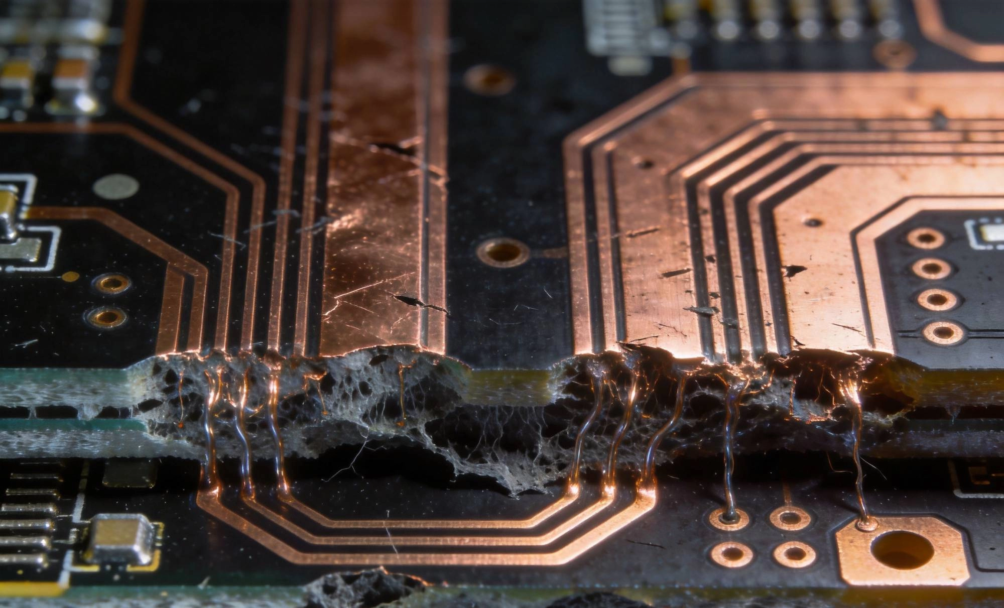
Conductive Anodic Filament formation represents one of the most insidious failure mechanisms in modern high-density printed circuit boards. Unlike solder joint fractures or component failures that announce themselves with visible symptoms, CAF fail...
https://www.high-density-interconnect-pcb.comhttps://www.high-density-interconnect-pcb.com/hdi-pcb-reliability/conductive-anodic-filament-caf-resistance-in-high-density-boards/
The aerospace industry stands at the forefront of electronic innovation, demanding reliability, performance, and miniaturization that push the boundaries of what printed circuit board technology can achieve. Flight control systems, navigation compu...
https://www.high-density-interconnect-pcb.comhttps://www.high-density-interconnect-pcb.com/automotive-ev-systems/the-role-of-hdi-in-avionics-and-flight-control-systems/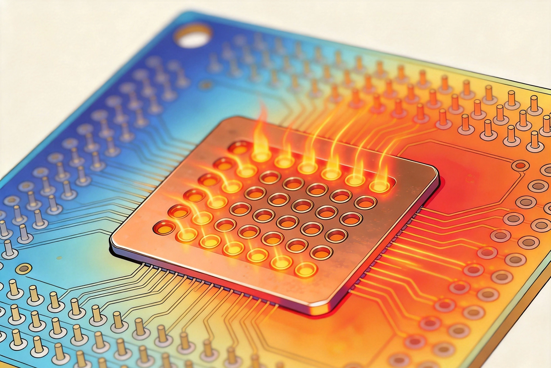
Via-in-pad — placing a via directly within a component land pad rather than beside it — is one of the most consequential design decisions in modern PCB layout. It affects thermal performance, solder joint integrity, manufacturing cost, and long-ter...
https://www.high-density-interconnect-pcb.comhttps://www.high-density-interconnect-pcb.com/hdi-pcb-thermal-management/the-impact-of-via-in-pad-on-thermal-performance-and-reliability/