
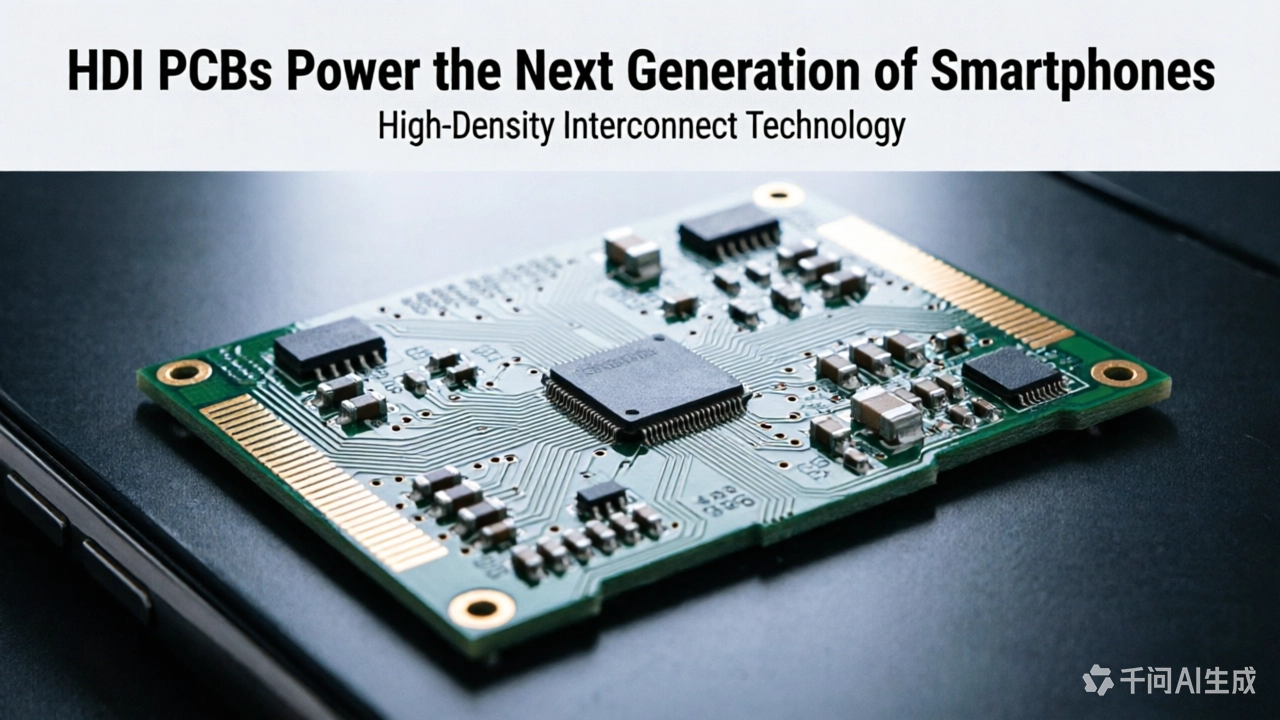
The smartphone in your pocket is a marvel of miniaturization. Within its slim profile, dozens of chips, thousands of components, and miles of copper traces work together to deliver computing power that would have seemed like science fiction just tw...
https://www.high-density-interconnect-pcb.comhttps://www.high-density-interconnect-pcb.com/energy-power-electronics/how-hdi-pcbs-power-the-next-generation-of-smartphones/
Open any smartphone, peel back the EMI shield, and look at the main PCB. What you see is a board roughly the size of a credit card carrying an application processor with 2,000+ solder balls on 0.35 mm pitch, 8–16 GB of LPDDR memory in a package-on-...
https://www.high-density-interconnect-pcb.comhttps://www.high-density-interconnect-pcb.com/energy-power-electronics/how-hdi-technology-enables-the-miniaturization-of-modern-electronics/